1.5. Test Results
The following table contains the possible results and their definition.
| Result | Definition |
|---|---|
| PASS | TheDevice Under Test (DUT) was observed to exhibit conformant behavior. |
| PASS with comments | TheDUT was observed to exhibit conformant behavior. However, an additional explanation of the situation is included, such as due to time limitations only a portion of the testing was performed. |
| FAIL | The DUT was observed to exhibit non-conformant behavior. |
| Warning | TheDUT was observed to exhibit behavior that is not recommended. |
| Refer to comments | From the observations, a valid pass or fail could not be determined. An additional explanation of the situation is included. |
The following table shows the results for test cases CGS.1, CGS.2, ILA.1, ILA.2, ILA.3, TL.1, and SCR.1 with different values of L, M, F, K, subclass, data rate, sampling clock, link clock and SYSREF frequencies.
| Test | L | M | F | SCR | K | Lane rate (Gbps) | Sampling Clock (GHz) | SYSREF pulse frequency (MHz) | Result |
|---|---|---|---|---|---|---|---|---|---|
| 1 | 1 | 2 | 4 | 0 | 32 | 12.5 | 5 | 9.765 | Pass |
| 2 | 1 | 2 | 4 | 1 | 32 | 12.5 | 5 | 9.765 | Pass |
| 3 | 2 | 2 | 2 | 0 | 32 | 12.5 | 5 | 19.5312 | Pass |
| 4 | 2 | 2 | 2 | 1 | 32 | 12.5 | 5 | 19.5312 | Pass |
| 5 | 3 | 2 | 4 | 0 | 32 | 12.5 | 3.75 | 9.765 | Pass |
| 6 | 3 | 2 | 4 | 1 | 32 | 12.5 | 3.75 | 9.765 | Pass |
| 7 | 4 | 2 | 1 | 0 | 32 | 12.5 | 5 | 39.0625 | Pass |
| 8 | 4 | 2 | 1 | 1 | 32 | 12.5 | 5 | 39.0625 | Pass |
| 9 | 6 | 2 | 2 | 0 | 32 | 12.5 | 3.75 | 19.5312 | Pass |
| 10 | 6 | 2 | 2 | 1 | 32 | 12.5 | 3.75 | 19.5312 | Pass |
| 11 | 8 | 1 | 1 | 0 | 32 | 12.5 | 5 | 39.0625 | Pass |
| 12 | 8 | 1 | 1 | 1 | 32 | 12.5 | 5 | 39.0625 | Pass |
| 13 | 8 | 2 | 1 | 0 | 32 | 12.5 | 5 | 39.0625 | Pass |
| 14 | 8 | 2 | 1 | 1 | 32 | 12.5 | 5 | 39.0625 | Pass |
The following table shows the results for test cases DL.1 and DL.2 with different values of L, M, F, K, subclass, lane rate, sampling clock, link clock and SYSREF pulse frequencies. Also DAC registers LMFCDel (LMFC offset) and LMFCVar (RBD offset) configured with values to achieve deterministic latencies are tabulated.
| S.no | L | M | F | Samplin g Clock (GHz) | LMFC Del | LMFC Var | SYSREF pulse frequency (MHz) | Total Latency Result |
|---|---|---|---|---|---|---|---|---|
| 1 | 1 | 2 | 4 | 5.0 | 0x1D | 0x4 | 9.765 | Pass (367.4-367.8 ns) |
| 2 | 2 | 2 | 2 | 5.0 | 0x8 | 0xA | 19.5312 | Pass (236.4-237.0 ns) |
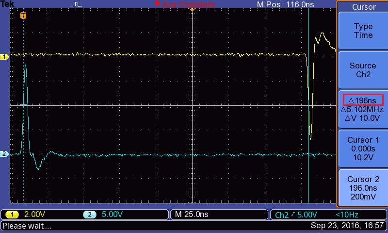
| 3 | 3 | 2 | 4 | 3.75 | 0x1D | 0x4 | 9.765 | Pass (195.6-196.4 ns) |
| 4 | 4 | 2 | 1 | 5.0 | 0 | 0x1F | 39.0625 | Pass (180.8-181.4 ns) |
| 5 | 6 | 2 | 2 | 3.75 | 0xD | 0x4 | 19.5312 | Pass (146.2-147.2 ns) |
| 6 | 8 | 1 | 1 | 5.0 | 0x6 | 0x4 | 39.0625 | Pass (119.6-120.6 ns) |
| 7 | 8 | 2 | 1 | 5.0 | 0x6 | 0x6 | 39.0625 | Pass (139.6-140.4 ns) |
Figure 5. Sine Wave at DAC Analog Channel OutputFigure shows the sine wave output from DAC analog channel.
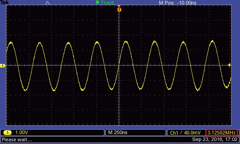
Figure 6. Deterministic Latency Measurement for LMF = 324 ConfigurationFigure shows the time difference between pulses in deterministic latency measurement for LMF = 324 Configuration