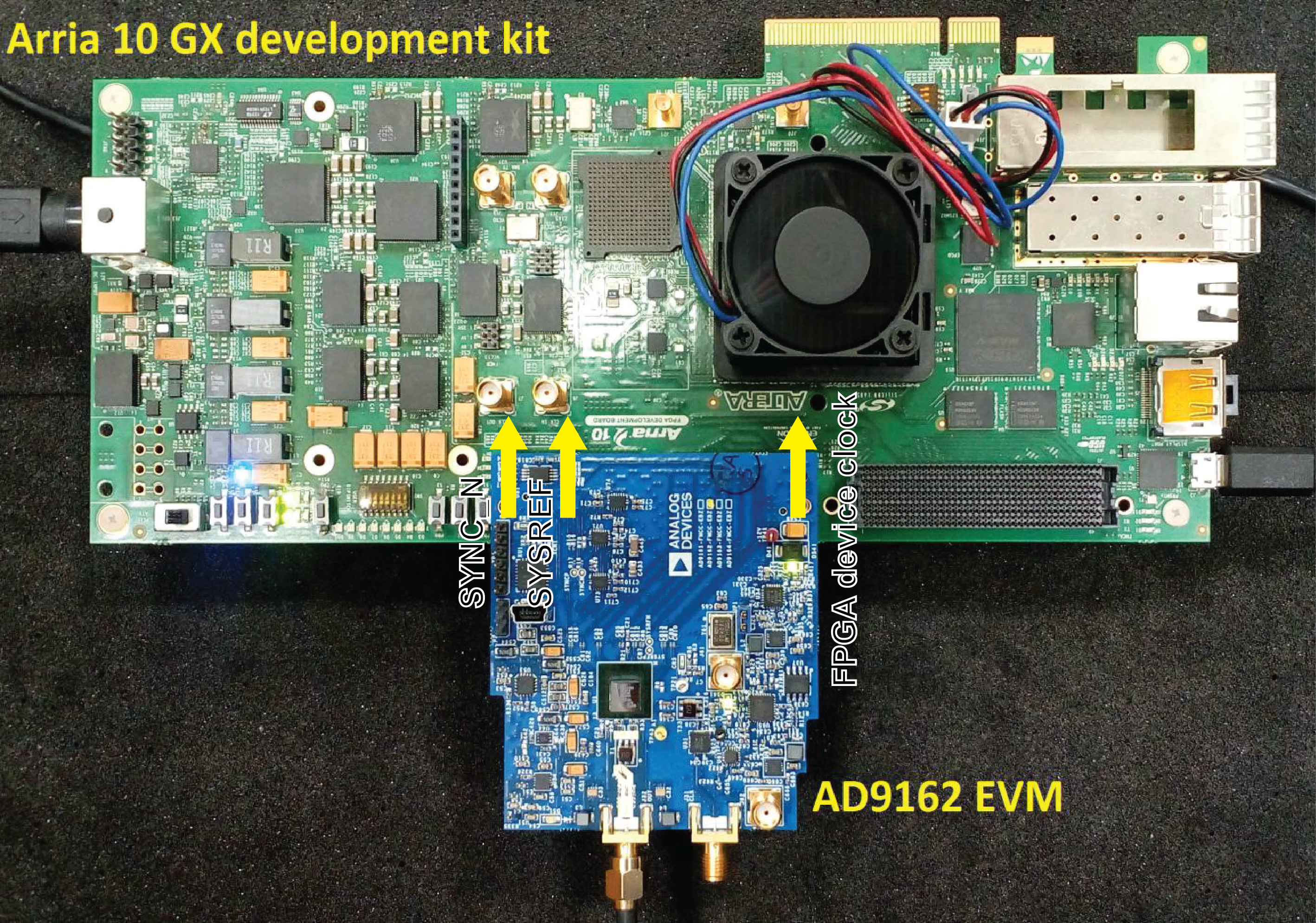
1.2. Hardware Setup
- The AD9162 EVM derives power from FMC pins.
- The DAC sampling clock is supplied by the ADF4355 clock generator on the DAC AD9162 EVM.
- The FPGA device clock is supplied by the AD9508 clock fan-out buffer on the EVM through FMC pins. The link and frame clocks are generated from the device clock using IOPLL.
- For subclass 1, AD9508 clock generator on the EVM generates SYSREF for JESD204B IP core through FMC pins as well as the DAC AD9162.
- The sync_n signal is transmitted from the DAC to FPGA through FMC.

In this setup, where LMF=821, the data rate of transceiver lanes is 12.5 Gbps. Two clock generators are available on the EVM – ADF4355 and AD9508. The ADF4355 clock generator uses 120MHz crystal oscillator as reference clock to generate the DAC sampling clock and reference clock for AD9508 clock generator. The AD9508 supplies FPGA device clock and SYSREF for FPGA through FMC pins. In addition to this SYSREF for DAC is also generated. The DAC AD9162 provides SYNC_N signal through FMC pins. The DAC operates in single JESD link in all configurations.
The clock generators and DAC are programmed by FPGA through SPI interface. The DAC provides a 4-wire SPI interface, while the clock generators on the EVM provide a 3-wire SPI interface for programming. The SPI word size is 24 bits for DAC and AD9508 while the word size is 32 bits for ADF4355 clock generator. A user logic is written on FPGA to take care of these differences and allow programming of all 3 SPI slaves.