A newer version of this document is available. Customers should click here to go to the newest version.
3.1. Methodology
This simulation emulates an Intel Stratix® V GX transmitter (with embedded package model), a PCI Express* 8GT receiver (with embedded package model), and a ~18-inch backplane channel. Per PCI Express* 8GT specifications, the link operates at 8 Gbps with a bit error rate (BER) < 10–12. The transmitter must have a minimum differential output voltage of 800 mV and a rise/fall time of ~35 ps (at 0.8 V VOD). In this simulation, the Stratix® V GX transmitter is set to 800 mV VOD (VOD level = 40). Additionally, the Stratix® V GX transmitter has a 4-tap FIR to compensate for channel effects. The PCI Express* 8G receiver has CTLE and a 1-Tap DFE per PCI-SIG definition.
To accomplish these goals, set up a transmitter model, a receiver model, and a link with the following parameters:
- Data rate: 8 Gbps
- Test pattern: PRBS-23
- BER target: BER < 10–12
- Stratix® V GX transmitter
- VOD: 800 mV (VOD Level = 40)
- Edge rate: Per Stratix® V GX characteristics
- 4-Tap TX FIR (1 pre-tap and 2 post-taps)
- Stratix® V GX package model (embedded)
- PLL: ATX (LC) set to low bandwidth
- Output Jitter: Retrieved from the Intel Characterization Database (embedded in Advanced Link Analyzer; contact My Intel support to enable this function)
- DCD = ~0.012 UI
- BUJ = ~0.032 UI
- RJ = ~1.00 psRMS (8 Gbps, BER < 10–12)
- Receiver
- CTLE:
- Programmable with 6 dB~12 dB boost at 4 GHz
- Per PCI-SIG specifications
- 1-tap DFE
- PCI-SIG receiver package model (12-port S-parameter model from PCI-SIG)
- CDR: Generic binary CDR with high loop bandwidth ~26 MHz
- Receiver Jitter:
- DJ = ~7 ps
- RJ = ~1.55 psRMS (at BER < 10–12)
- CTLE:
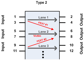
The ~18-inch backplane channel is described by a 12-port S-parameter model. The S-parameter is measured (or generated) with port configuration type 2, as shown in the following figure:
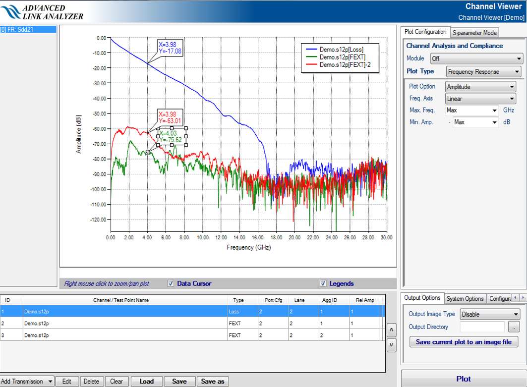
The Advanced Link Analyzer Channel Viewer shows that the backplane channel has approximately 17.15 dB loss at 4 GHz. The PCI-SIG RX package has 3.5 dB insertion loss at 4 GHz. The overall link has about 21 dB of loss (as shown in the Combined Channel black curve, not including Stratix® V GX transmitter package) at 4 GHz, which requires heavy TX and RX equalizations to achieve the required BER target.
For comparative purposes, the following table and figure show a typical external 100 MHz transmitter reference clock with measured phase noise characteristics and spurs at three different frequencies.
| Phase Noise |
Spurs |
||
|---|---|---|---|
| Frequency |
Phase Noise (dBc) |
Frequency |
Amplitude (dBc) |
| 10 Hz |
–68 |
100 kHz |
–80 |
| 100 Hz |
–82 |
1 MHz |
–90 |
| 1 kHz |
–84 |
10 MHz |
–96 |
| 1 MHz and above |
–140 |
||
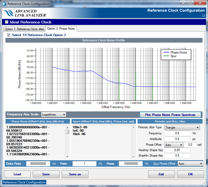
The PLL in the Stratix® V GX transmitter is enabled using ATX (LC) with low bandwidth configuration. The PLL effectively reduces the noise effects from the external reference clock.
Use the Advanced Link Analyzer’s link optimization algorithm to find the optimal equalization settings for both the transmitter and receiver. In this demonstration, you use the CTLE=>FIR+DFE link optimization method.