A newer version of this document is available. Customers should click here to go to the newest version.
1. Answers to Top FAQs
2. Overview of the Intel® FPGA Power and Thermal Calculator
3. Estimating Power Consumption with the Intel® FPGA Power and Thermal Calculator
4. Intel® FPGA Power and Thermal Calculator Graphical User Interface
5. Intel® FPGA Power and Thermal Calculator Pages
6. Factors Affecting the Accuracy of the Intel® FPGA PTC
7. Intel® FPGA Power and Thermal Calculator User Guide Archive
8. Document Revision History for the Intel® FPGA Power and Thermal Calculator User Guide
A. Measuring Static Power
5.1. Intel® FPGA PTC - Power Summary
5.2. Intel® FPGA PTC - Common Page Elements
5.3. Intel® FPGA PTC - Main Page
5.4. Intel® FPGA PTC - Logic Page
5.5. Intel® FPGA PTC - RAM Page
5.6. Intel® FPGA PTC - DSP Page
5.7. Intel® FPGA PTC - Clock Page
5.8. Intel® FPGA PTC - PLL Page
5.9. Intel® FPGA PTC - I/O Page
5.10. Intel® FPGA PTC - I/O-IP Page
5.11. Intel® FPGA PTC - Transceiver Page
5.12. Intel® FPGA PTC - HPS Page
5.13. Intel® FPGA PTC - Crypto Page
5.14. Intel® FPGA PTC - HBM Page
5.15. Intel® FPGA PTC - Thermal Page
5.16. Intel® FPGA PTC - Report Page
5.10. Intel® FPGA PTC - I/O-IP Page
Each row in the I/O-IP page of the Intel® FPGA Power and Thermal Calculator (PTC) represents a design module. You can use the I/O-IP page to specify the properties of external memory interface and HPS IPs supported by the target device.
Figure 29. I/O-IP Page of the Intel® FPGA PTC
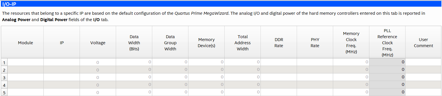
The I/O-IP page populates other Intel® FPGA PTC pages with resources used by a selected IP. Analog I/O power and digital power of hard memory controllers and HPS IPs that you enter on this page are reported in the Analog Power and Digital Power fields of the I/O-IP page. If the IP uses other resource types (for example Logic or PLL), the power is reported on the corresponding data entry page.
I/O-IP Page Information
| Column Heading | Description |
|---|---|
| Module | Specifies a name for the IP in this column. The module name depends on the selected IP type. It helps to cross-reference each IP module and its corresponding auto-populated entries on other pages. This name is auto-populated when IP type is selected in the IP column and cannot be changed. |
| IP | Specifies the type of the IP in the design. |
| Voltage | Specifies the I/O voltage of the signaling between periphery device and interface. |
| Data Width (Bits) | Specifies the interface data width of the specific IP (in bits). |
| # of DQS Groups | Specifies the number of DQS groups. |
| Memory Device(s) | Specifies the number of memory devices connected to the interface. |
| Total Address Width | Specifies the total address width. This value is used to derive the total number of address pins required. |
| DDR Rate | Specifies the clock rate of user logic. Determines the clock frequency of user logic in relation to the memory clock frequency. For example, if the memory clock sent from the FPGA to the memory device is toggling at 800MHz, a "Quarter rate" interface means that the user logic in the FPGA runs at 200MHz. |
| PHY Rate | Specifies the clock rate of PHY logic. Determines the clock frequency of PHY logic in relation to the memory clock frequency. For example, if the memory clock sent from the FPGA to the memory device is toggling at 800MHz, a "Quarter rate" interface means that the PHY logic in the FPGA runs at 200MHz. |
| Memory Clock Frequency (MHz) | Specifies the frequency of memory clock (in MHz). |
| PLL Reference Clock Frequency (MHz) | Reports the PLL Reference Clock Frequency (in MHz). |
| User Comments | Enter any comments. This is an optional entry. |