1. Stratix® 10 Embedded Memory Overview
2. Stratix® 10 Embedded Memory Architecture and Features
3. Stratix® 10 Embedded Memory Design Considerations
4. Stratix® 10 Embedded Memory IP References
5. Stratix 10 Embedded Memory Design Example
6. Stratix® 10 Embedded Memory User Guide Archives
7. Document Revision History for the Stratix® 10 Embedded Memory User Guide
2.1. Byte Enable in Stratix® 10 Embedded Memory Blocks
2.2. Address Clock Enable Support
2.3. Asynchronous Clear and Synchronous Clear
2.4. Memory Blocks Error Correction Code (ECC) Support
2.5. Force-to-Zero
2.6. Coherent Read Memory
2.7. Freeze Logic
2.8. True Dual Port Dual Clock Emulator
2.9. 'X' Propagation Support in Simulation
2.10. Stratix® 10 Supported Embedded Memory IPs
2.11. Stratix® 10 Embedded Memory Clocking Modes
2.12. Stratix® 10 Embedded Memory Configurations
2.13. Initial Value of Read and Write Address Registers
3.1. Consider the Memory Block Selection
3.2. Consider the Concurrent Read Behavior
3.3. Read-During-Write (RDW)
3.4. Consider Power-Up State and Memory Initialization
3.5. Reduce Power Consumption
3.6. Avoid Providing Non-Deterministic Input
3.7. Avoid Changing Clock Signals and Other Control Signals Simultaneously
3.8. Including the Reset Release FPGA IP in Your Design
3.9. Resource and Timing Optimization Feature in MLAB Blocks
3.10. Consider the Memory Depth Setting
3.11. Consider Registering the Memory Output
4.1.1. Release Information for RAM and ROM IPs
4.1.2. RAM: 1-PORT FPGA IP Parameters
4.1.3. RAM: 2-PORT FPGA IP Parameters
4.1.4. RAM: 4-PORT FPGA IP Parameters
4.1.5. ROM: 1-PORT FPGA IP Parameters
4.1.6. ROM: 2-PORT FPGA IP Parameters
4.1.7. RAM and ROM Interface Signals
4.1.8. Changing Parameter Settings Manually
4.3.1. Release Information for FIFO FPGA IP
4.3.2. Configuration Methods
4.3.3. Specifications
4.3.4. FIFO Functional Timing Requirements
4.3.5. SCFIFO ALMOST_EMPTY Functional Timing
4.3.6. FIFO Output Status Flag and Latency
4.3.7. FIFO Metastability Protection and Related Options
4.3.8. FIFO Synchronous Clear and Asynchronous Clear Effect
4.3.9. SCFIFO and DCFIFO Show-Ahead Mode
4.3.10. Different Input and Output Width
4.3.11. DCFIFO Timing Constraint Setting
4.3.12. Coding Example for Manual Instantiation
4.3.13. Design Example
4.3.14. Gray-Code Counter Transfer at the Clock Domain Crossing
4.3.15. Guidelines for Embedded Memory ECC Feature
4.3.16. FIFO IP Parameters
4.3.17. Reset Scheme
4.3.9. SCFIFO and DCFIFO Show-Ahead Mode
You can set the read request (rdreq) signal read access behavior by selecting normal or show-ahead mode.
For normal mode, the FIFO IP treats the rdreq port as a normal read request that only performs read operation when the port is asserted.
For show-ahead mode, the FIFO IP treats the rdreq port as a read-acknowledge that automatically outputs the first word of valid data in the FIFO IP (when the empty is low) without asserting the rdreq signal. Asserting the rdreq signal causes the FIFO IP to output the next data word, if available.
Figure 40. Normal Mode Waveform 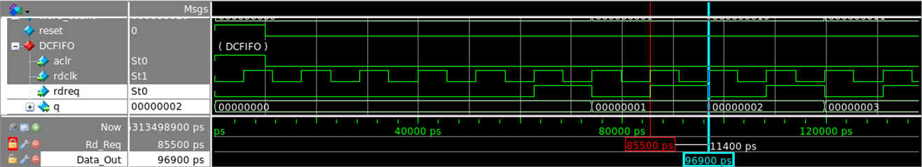
Data appears after the rdreq asserted.
Figure 41. Show-Ahead Mode Waveform 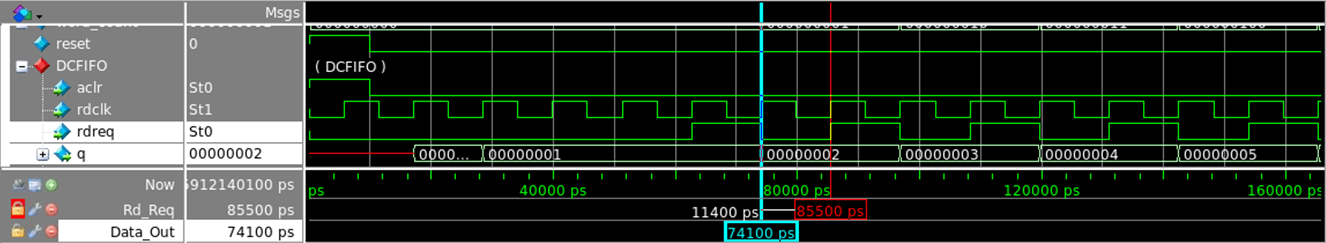
Data appears before the rdreq asserted.