1.3. DAC3XJ8XEVM Software Setup
The DAC3XJ8XEVM software configures the DAC37J84 device and LMK04828 clock generator for JESD204B link operation.
- Configure the FPGA.
- In the Quick Start tab, select a value for DAC Data Input Rate, Number of SerDes Lanes, and Interpolation options to meet the settings as stated in Table. The DAC device clock is synonymous to the DAC Output Rate.
- Click the 1. Program LMK04828 and DAC3XJ8X button.
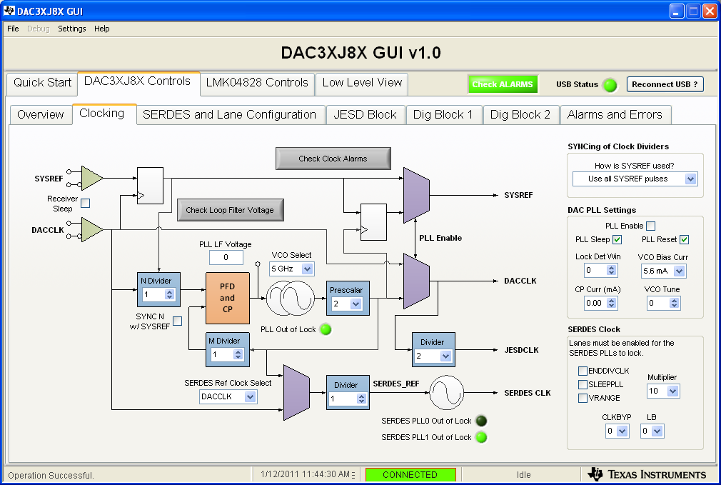
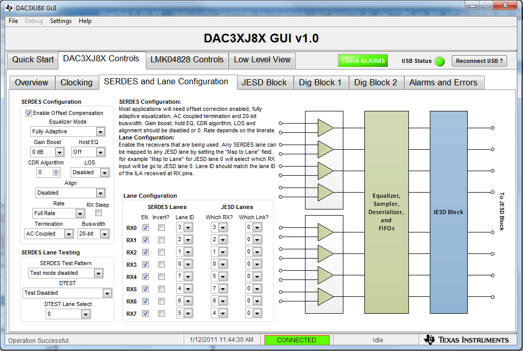
- In the DAC3XJ8X Controls tab, select the Clocking sub tab. For the SYNCing of Clock Dividers drop-down list, select Use all SYSREF pulses.
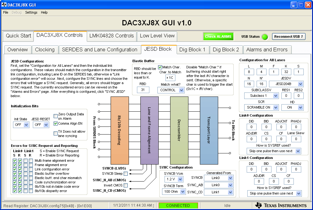
- In the DAC3XJ8X Controls tab, select the JESD Block sub tab.
- At the Elastic Buffer section, turn on the Match Char. checkbox.
- At the Initialization Bits section, turn off the TX Does not allow lane syncing checkbox.
- Change the K and RBD value accordingly. RBD value is K value minus 1. For example, when K = 32, set RBD = 31.
- At the Configuration for All Lanes section, for the SCR drop-down list, select SCRAMBLE ON if scrambler is turned on at the JESD204B IP core. Select SCRAMBLE OFF if scrambler is turned off at the JESD204B IP core.
- At the Errors for SYNC Request and Reporting section, under the Link0 S column, turn on the Link configuration error, 8b/10b not-in-table code error, and 8b/10b disparity error checkboxes. Optionally, you can turn off all the checkboxes under the Link1 S R columns.
- In the LMK04828 Controls tab, select the SYSREF and SYNC sub tab.
- At the FPGA Clock and SYSREF section, turn on the HS checkbox for DCLK Delay.
- At the SYSREF Configuration section, change the SYSREF Divider value according to the mode and K value of the targeted operation:
- LMFS=148, K=16 and 32, SYSREF Divider=768
- LMFS=244, K=16 and 32, SYSREF Divider=512
- LMFS=4421, K=16 and 32, SYSREF Divider=256
- LMFS=8411, K=20, SYSREF Divider=80
- LMFS=8411, K=32, SYSREF Divider=128
- For the SYSREF Source drop-down list, select Normal SYNC.
- At the SYNC Configuration section, set the following:
- For the SYNC Mode drop-down list, select Pin.
- Turn off the SYSREF SYNC Disable, DCLKout0 SYNC Disable, and DCLKout2 SYNC Disable checkboxes.
- Turn on the SYNC Pin Polarity checkbox. Then turn off this option.
- Turn on the SYSREF SYNC Disable, DCLKout0 SYNC Disable, and DCLKout2 SYNC Disable checkboxes.
- At the SYSREF Configuration section, for the SYSREF Source drop-down list, select SYSREF Pulses.
- In the Quick Start tab, click the 2. Reset DAC JESD Core button. Then, click the 3. Trigger LMK04828 SYSREF button
You can record steps 4 to 6 in a log file for future replay. Double-click the lower left corner (see Figure 3) of the software. A pop-up Status Log window is launched. Right click at the empty area and select "Clear Log" and close the pop-up window. Perform steps 4 to 6. Re-open the pop-up window and select the series of actions that are recorded. Right click at the empty area and save the selected actions into a file with .cfg extension. Use an editor to delete the read register records. Then transform the write register records into the format as indicated in the sample setup files that are included in the graphical user interface (GUI) installation. A sample configuration file for the LMF=841, K=32, RBD=31, SCR=1 is shown below.
DAC3XJ8X
0x51 0x00FF //enable sync request for link 0
0x54 0x0000 //disable sync request for link 1
0x55 0x0000 //disable error reporting for link 1
0x4F 0x1CC1 //turn on lane sync, match specific character 0x1C to start JESD buffering
0x4C 0x1F07 //K=32, L=8
0x4B 0x1E00 //RBD=31, F=1
0x4E 0x0F6F //SCR=1, HD=1
0x24 0x0010 //cdrvser_sysref_mode=use all sysref pulses

LMK04828
0x13A 0x00 //sysref divider=128
0x13B 0x80 //sysref divider=128
0x104 0x60 //half step for FPGA device clk
0x139 0x00 //set SYSREF_Mux to "Normal"
0x143 0x11 // trigger SYNC event using "Pin" mode
0x144 0x00 //enable syncing of all clock outputs
0x143 0x31 //toggle SYNC Pin Polarity bit
0x143 0x11 //toggle SYNC Pin Polarity bit
0x144 0xFF //disable syncing of all clock outputs
0x139 0x02 //set SYSREF_MUX to "Pulses"
The figures below show the examples of GUI setup for LMF = 841 configuration.
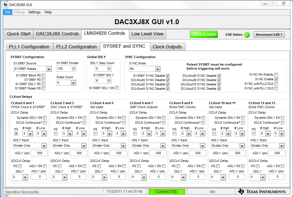
- CLKout0 supplies device clock to the FPGA.
- CLKout1 is configured as the SYSREF source for the FPGA.
- CLKout2 supplies device clock to the DAC.
- CLKout3 is configured as the SYSREF source for the DAC.
To perform short transport layer test, you must properly set up the pattern checker at DAC transport layer according to the following steps:
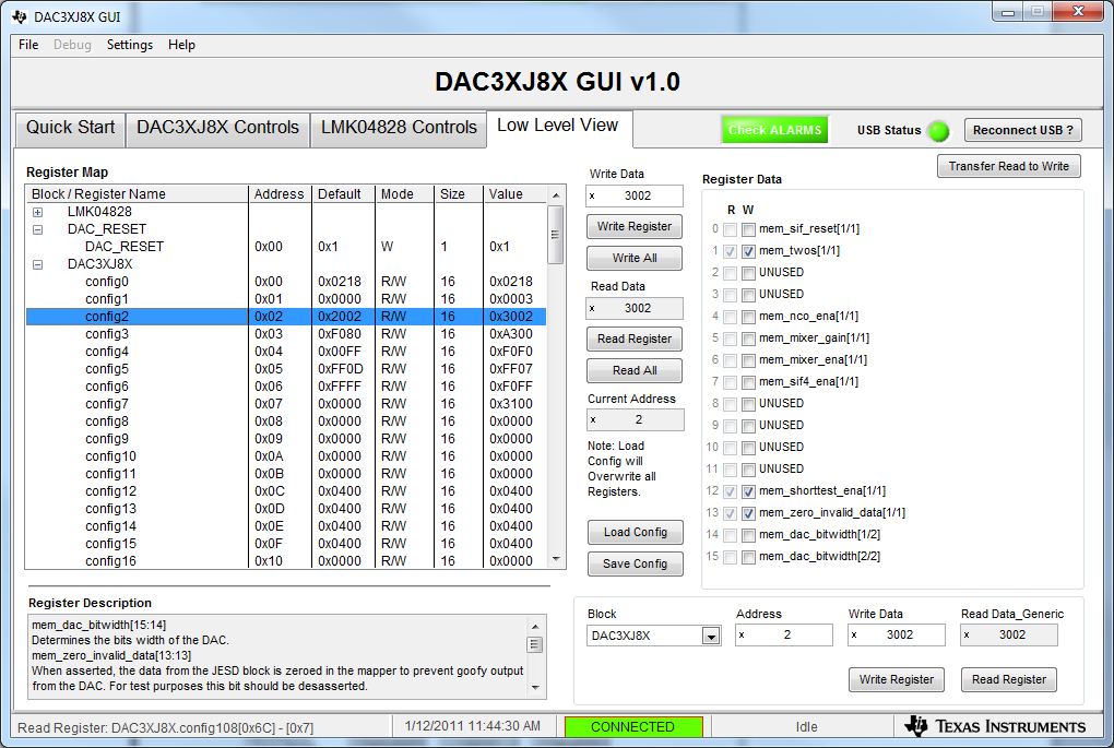
- Set bit 12 of the config2 register (address 0x02) to enable short transport layer checker. To do this, highlight the config2 register and check the bit 12 checkbox in the “DAC3XJ8X Controls > Low Level View” tab. Click the Write Register button to write the setting to the SPI interface of the DAC37J84.
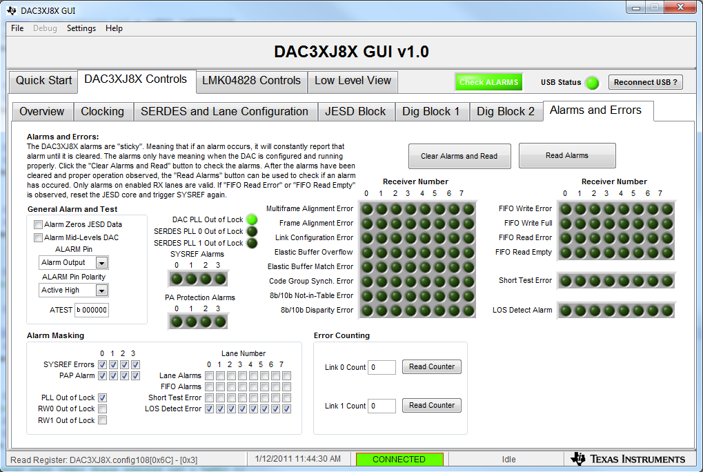
- Clear bits 8–15 of the config6 register (address 0x06) to disable the “Short Test Error” alarm mask. Clear the bits according to the respective active lanes (for example, bit 8 is for lane0, bit 15 is for lane 7). To do this, uncheck the Short Test Error checkboxes at the Alarm Masking section in the “DAC3XJ8X Controls > Alarms and Errors” tab.
- Set the FPGA to output the corresponding test pattern, according to the parameter configuration listed in Table.
- Check the result at bits 8–15 of the config109 register. To do this, press the Clear Alarms and Read button in the “DAC3XJ8X Controls > Alarms and Errors” tab and monitor the Short Test Error indicator.