Generic Serial Flash Interface Intel® FPGA IP User Guide
ID
683419
Date
4/01/2024
Public
A newer version of this document is available. Customers should click here to go to the newest version.
1.1. Release Information
1.2. Device Family Support
1.3. Signals
1.4. Parameters
1.5. Register Map
1.6. Using Generic Serial Flash Interface Intel® FPGA IP
1.7. Generic Serial Flash Interface Intel® FPGA IP Reference Design
1.8. Flash Access Using the Generic Serial Flash Interface Intel® FPGA IP
1.9. Intel HAL Driver
1.10. Generic Serial Flash Interface Intel® FPGA IP User Guide Archives
1.11. Document Revision History for the Generic Serial Flash Interface Intel® FPGA IP User Guide
1.7.3. Creating Nios® II Hardware System
- In the Quartus® Prime software, go to File > New Project Wizard.
- Create a new Quartus® Prime Prime project named generic_flash_access in a new directory and select the Cyclone V E 5CEFA7F3117 device.
- Select Tools > Platform Designer, and save the file as generic_flash_access.qsys.
- Double-click on the clock source clk_0 and change the Clock frequency to 100000000 Hz (100MHz).
- Right click on clk_0 and rename it as sys_clk.
- Add a Nios® II processor:
- Go to Processor and Peripherals > Embedded Processors > Nios II Processor, and click Add.
- Click Finish to add the Nios® II processor to the design and rename it as nios2.
Note: Ignore any messages about parameters that have not been specified yet.
- Add a Generic Serial Flash Interface IP:
- Select Basic Functions > Configuration and Programming > Generic Serial Flash Interface Intel FPGA IP, and click Add. Rename this component as intel_generic_serial_flash_interface_top0.
- Set the device density.
Note: This reference design uses 1024MB flash device density.
- Connect data_master of processor to avl_mem and avl_csr, and instruction_master of processor to only avl_mem of this component.
- Add an On-chip Memory IP:
- Select Basic Functions > On Chip Memory > On-Chip Memory (RAM or ROM) Intel FPGA IP.
- Set the Total Memory Size to 40960 bytes (40 KBytes).
- Click Finish and rename as main_memory.
- Connect its slave to data_master and instruction_master of processor.
- Add a JTAG UART IP:
- Go to Interface Protocols > Serial > JTAG UART Intel FPGA IP, and click Add.
- Click Finish and rename it as jtag_uart.
- Connect its avalon_jtag_slave port to the data_master port of the processor.
- In the IRQ column, connect the interrupt sender port from the Avalon_jtag_slave port to the interrupt receiver port of the processor and type 0.
- Connect clock input of sys_clk to clock input of all other components.
- Resolve all Nios® II processor error messages before generating the Platform Designer system:
- Double click the Nios® II processor nios2.
- Click Vectors, change both the Reset vector memory and Exception vector memory to main_memory.s1.
- Click System tab and click on the drop-down menu System and click Assign Base Address to auto assign base addresses for all the components.
- Under the same menu, click Create Global Reset Network to connect the reset signals to form a global reset network.
Figure 7. Completed Platform Designer Connection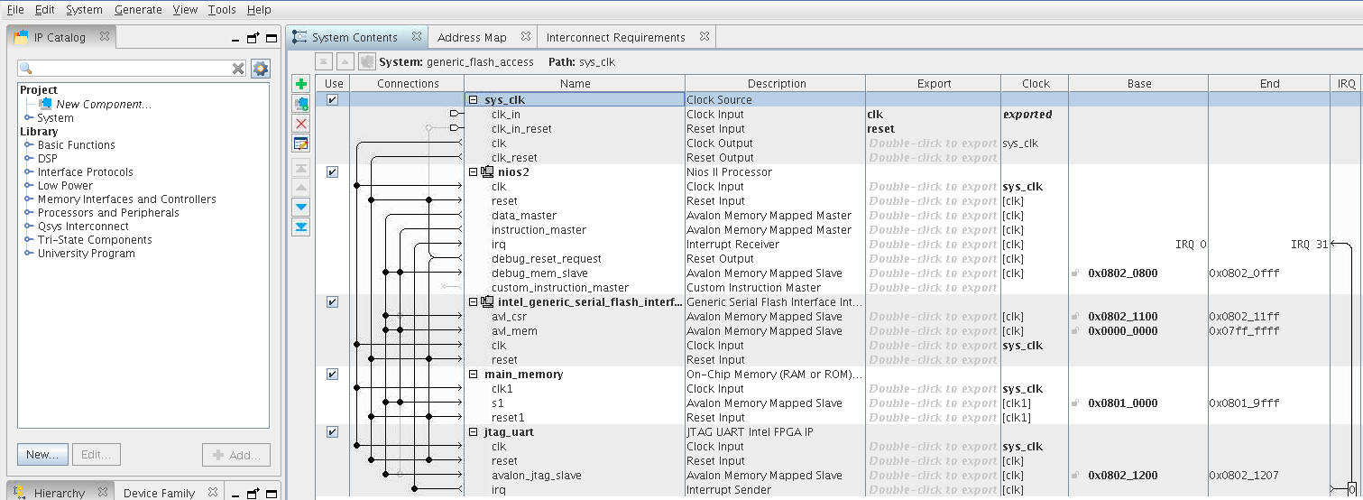
- Generate the system:
- Click Generate HDL on the bottom of the window.
- When completed, the Platform Designer displays Generate: Completed successfully.