F-Tile Avalon® Streaming Intel® FPGA IP for PCI Express* Design Example User Guide
ID
683372
Date
7/14/2022
Public
A newer version of this document is available. Customers should click here to go to the newest version.
3.3.1.4. Performance Design Example Testbench
The figure below shows the Performance design example simulation design hierarchy. The tests for the Performance design example are defined with the apps_type_hwtcl parameter set to 3. The tests run under this parameter value are defined in ebfm_cfg_rp_ep_rootport, find_mem_bar and perf_ed_dma_write/perf_ed_dma_read.
Figure 25. Performance Design Example Simulation Design Hierarchy
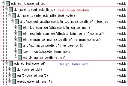
The testbench starts with link training and then accesses the configuration space of the IP for enumeration. A task called perf_ed_dma_write and perf_ed_dma_read (defined in the Root Port PCIe BFM altpcietb_bfm_rp_gen4_x16.sv) then performs the PCIe link test. This test consists of the following steps:
- Issue a memory write command to set up the Performance design example's target memory write address.
- Issue a memory write command to trigger the Performance design example to send 10 memory writes with 128 bytes in length.
- Issue a memory write command to set up the Performance design example's target memory read address.
- Issue a memory write command to trigger the Performance design example to send 10 memory reads with 128 bytes in length.
The first memory write takes place around 208 µs. The 10 memory writes and 10 memory reads with completions from the RP BFM appear shortly after the memory write requests at the Avalon-ST RX interface.