F-Tile Avalon® Streaming Intel® FPGA IP for PCI Express* Design Example User Guide
ID
683372
Date
7/14/2022
Public
A newer version of this document is available. Customers should click here to go to the newest version.
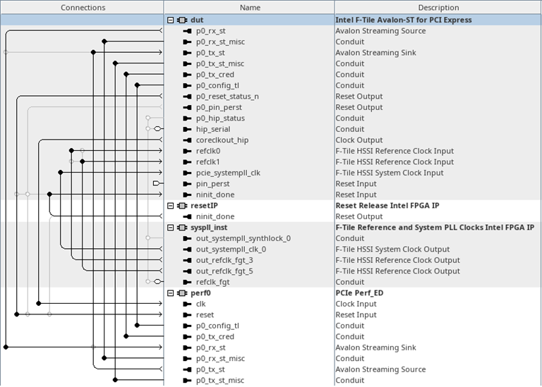
2.3.1. Performance Design Example Functional Description
- The generated F-Tile Avalon Streaming Hard IP Endpoint variant (DUT) with the parameters you specified. This component interacts with the root complex/switch at the other end of the PCIe link and translates the data from the PCIe link into Avalon-ST data format, and vice versa.
- The PCIe Perf_ED (perf0) component generates the requested data traffic for throughput measurement. It consists of the following sub-modules:
- The pioperf_multitlp_adapter (Avalon-ST Interface Adapter) module converts the 2-segment data of the Avalon-ST interface into two single segment streams of Avalon-ST data.
- The pioperf_rx_diverter module diverts memory write or memory read TLPs from the host and completion TLPs to their respective destinations for further processing.
- The pioperf_rx_intf (RX Interface) module decodes the TLP headers and data from the pioperf_rx_diverter module. It also extracts the information needed to construct the TLP header of the completion data such as the requester ID, tag, attribute, tc and byte count and then pass this to pioperf_tx_intf for further processing.
- The pioperf_tx_intf (TX Interface) module converts the requests from the pioperf_rx_intf and pioperf_dma_top modules into TLPs and send them to the F-Tile Avalon Streaming Hard IP. It transmits TLPs in a simplified weighted round-robin manner with this priority scheme: completion TLP > memory read TLP > memory write TLP.
- The pioperf_dma_top (DMA_TOP) module generates memory write and memory read requests and passes them to the pioperf_tx_intf module based on the information in the control register. Every memory read request will be tagged to expecting completion data before timeout to ensure data completeness. The release of memory write and memory read TLPs will build up the traffic at the TX and RX interfaces of the PCIe link. A throughput counter is included to analyze the overall throughput of the system.
- F-Tile Reference and System PLL Clocks IP: This IP is required for F-Tile PCIe interface implementation to configure the reference clock for the FGT PMA and System PLL. The clock from this IP is a logical connection. It is physically inside the F-Tile Avalon-ST IP for PCI Express Hard IP. There is no clock gating requirement at the design example level. The main clock of the PIO design example originates from coreclkout_hip of F-Tile Avalon-ST IP for PCI Express Hard IP running at 500 MHz. The clock originates from System PLL. This IP is required for F-Tile PCIe interface implementation to configure the reference clock for the FGT PMA and System PLL.
- Reset Release IP: This IP holds the control circuit in reset until the device has fully entered user mode. The FPGA asserts the INIT_DONE output to signal that the device is in user mode. The Reset Release IP generates an inverted version of the internal INIT_DONE signal to create the nINIT_DONE output that you can use for your design. The nINIT_DONE signal is high until the entire device enters user mode. After nINIT_DONE asserts (low), all logic is in user mode and operates normally. You can use the nINIT_DONE signal in one of the following ways:
- To gate an external or internal reset.
- To gate the reset input to the transceiver and I/O PLLs.
- To gate the write enable of design blocks such as embedded memory blocks, state machine, and shift registers.
- To synchronously drive register reset input ports in your design.
Figure 14. Platform Designer System Contents for F-Tile Avalon-ST for PCI Express 1x16 Performance Design Example