1. Introduction
2. Avalon® -ST Serial Peripheral Interface Core
3. SPI Core
4. SPI Agent/JTAG to Avalon® Host Bridge Cores
5. Intel eSPI Agent Core
6. eSPI to LPC Bridge Core
7. Ethernet MDIO Core
8. Intel FPGA 16550 Compatible UART Core
9. UART Core
10. Lightweight UART Core
11. JTAG UART Core
12. Intel FPGA Avalon® Mailbox Core
13. Intel FPGA Avalon® Mutex Core
14. Intel FPGA Avalon® I2C (Host) Core
15. Intel FPGA I2C Agent to Avalon® -MM Host Bridge Core
16. EPCS/EPCQA Serial Flash Controller Core
17. Intel FPGA Serial Flash Controller Core
18. Intel FPGA Serial Flash Controller II Core
19. Intel FPGA Generic QUAD SPI Controller Core
20. Intel FPGA Generic QUAD SPI Controller II Core
21. Interval Timer Core
22. Intel FPGA Avalon FIFO Memory Core
23. On-Chip Memory (RAM and ROM) Intel FPGA IP
24. On-Chip Memory II (RAM or ROM) Intel FPGA IP
25. PIO Core
26. PLL Cores
27. DMA Controller Core
28. Modular Scatter-Gather DMA Core
29. Scatter-Gather DMA Controller Core
30. Video Sync Generator and Pixel Converter Cores
31. Intel FPGA Interrupt Latency Counter Core
32. Performance Counter Unit Core
33. Vectored Interrupt Controller Core
34. System ID Peripheral Core
35. Intel FPGA GMII to RGMII Converter Core
36. HPS GMII to RGMII Adapter IP
37. Intel FPGA MII to RMII Converter Core
38. HPS GMII to TSE 1000BASE-X/SGMII PCS Bridge Core IP
39. Intel FPGA HPS EMAC to Multi-rate PHY GMII Adapter Core
40. Intel FPGA MSI to GIC Generator Core
41. Cache Coherency Translator IP
42. Altera ACE5-Lite Cache Coherency Translator
8.2.1. Unsupported Features
8.2.2. Interface
8.2.3. General Architecture
8.2.4. 16550 UART General Programming Flow Chart
8.2.5. Configuration Parameters
8.2.6. DMA Support
8.2.7. FPGA Resource Usage
8.2.8. Timing and Fmax
8.2.9. Avalon® -MM Agent
8.2.10. Over-run/Under-run Conditions
8.2.11. Hardware Auto Flow-Control
8.2.12. Clock and Baud Rate Selection
14.5.2.1. Transfer Command FIFO (TFR_CMD)
14.5.2.2. Receive Data FIFO (RX_DATA)
14.5.2.3. Control Register (CTRL)
14.5.2.4. Interrupt Status Enable Register (ISER)
14.5.2.5. Interrupt Status Register (ISR)
14.5.2.6. Status Register (STATUS)
14.5.2.7. TFR CMD FIFO Level (TFR CMD FIFO LVL)
14.5.2.8. RX Data FIFO Level (RX Data FIFO LVL)
14.5.2.9. SCL Low Count (SCL LOW)
14.5.2.10. SCL High Count (SCL HIGH)
14.5.2.11. SDA Hold Count (SDA HOLD)
22.6.1. altera_avalon_fifo_init()
22.6.2. altera_avalon_fifo_read_status()
22.6.3. altera_avalon_fifo_read_ienable()
22.6.4. altera_avalon_fifo_read_almostfull()
22.6.5. altera_avalon_fifo_read_almostempty()
22.6.6. altera_avalon_fifo_read_event()
22.6.7. altera_avalon_fifo_read_level()
22.6.8. altera_avalon_fifo_clear_event()
22.6.9. altera_avalon_fifo_write_ienable()
22.6.10. altera_avalon_fifo_write_almostfull()
22.6.11. altera_avalon_fifo_write_almostempty()
22.6.12. altera_avalon_write_fifo()
22.6.13. altera_avalon_write_other_info()
22.6.14. altera_avalon_fifo_read_fifo()
22.6.15. altera_avalon_fifo_read_other_info()
23.1. Core Overview
23.2. Component-Level Design for On-Chip Memory
23.3. Platform Designer System-Level Design for On-Chip Memory
23.4. Simulation for On-Chip Memory
23.5. Quartus® Prime Project-Level Design for On-Chip Memory
23.6. Board-Level Design for On-Chip Memory
23.7. Example Design with On-Chip Memory
23.8. On-Chip Memory (RAM and ROM) Intel FPGA IP Revision History
24.1. Core Overview
24.2. Embedded Memory Architecture and Features
24.3. Component-Level Configurations
24.4. Interface Signals
24.5. Control and Status Registers
24.6. Software Programming Model
24.7. Platform Designer System-Level Design for On-Chip Memory II
24.8. Simulation for On-Chip Memory II
24.9. Quartus® Prime Project-Level Design for On-Chip Memory II
24.10. Board-Level Design for On-Chip Memory II
24.11. Example Design with On-Chip Memory II
24.12. On-Chip Memory II (RAM and ROM) Intel FPGA IP Revision History
28.1. Core Overview
28.2. Feature Description
28.3. mSGDMA Descriptors
28.4. mSGDMA Descriptors with Prefetcher
28.5. mSGDMA IP Interface
28.6. mSGDMA Interrupt
28.7. Register Map of mSGDMA
28.8. Parameters
28.9. mSGDMA Programming Model
28.10. mSGDMA Prefetcher Programming Model
28.11. Driver Implementation
28.12. Example Code Using mSGDMA Core
28.13. Modular Scatter-Gather DMA Prefetcher Core
28.14. Modular Scatter-Gather DMA Dispatcher Core
28.15. Modular Scatter-Gather DMA Write Master Core
28.16. Modular Scatter-Gather DMA Read Master Core
28.17. Modular Scatter-Gather DMA Core Revision History
28.7.1. Status Register (Offset 0x0)
28.7.2. Control Register (Offset 0x4)
28.7.3. Read and Write Fill Level Register (Offset 0x8)
28.7.4. Response Fill Level Register (Offset 0xC)
28.7.5. Sequence Number Register (Offset 0x10)
28.7.6. Component Configuration 1 Register (Offset 0x14)
28.7.7. Component Configuration 2 Register (Offset 0x18)
28.7.8. Component Specification Register (Offset 0x1C)
28.7.9. Response Register (when MM response port is enabled)
28.7.10. Prefetcher Register
28.11.1. alt_msgdma_standard_descriptor_async_transfer
28.11.2. alt_msgdma_extended_descriptor_async_transfer
28.11.3. alt_msgdma_standard_descriptor_sync_transfer
28.11.4. alt_msgdma_extended_descriptor_sync_transfer
28.11.5. alt_msgdma_descriptor_sync_transfer
28.11.6. alt_msgdma_construct_standard_st_to_mm_descriptor
28.11.7. alt_msgdma_construct_standard_mm_to_st_descriptor
28.11.8. alt_msgdma_construct_standard_mm_to_mm_descriptor
28.11.9. alt_msgdma_construct_extended_st_to_mm_descriptor
28.11.10. alt_msgdma_construct_extended_mm_to_st_descriptor
28.11.11. alt_msgdma_construct_extended_mm_to_mm_descriptor
28.11.12. alt_msgdma_construct_prefetcher_standard_mm_to_mm_descriptor
28.11.13. alt_msgdma_construct_prefetcher_standard_st_to_mm_descriptor
28.11.14. alt_msgdma_construct_prefetcher_standard_mm_to_st_descriptor
28.11.15. alt_msgdma_construct_prefetcher_extended_mm_to_mm_descriptor
28.11.16. alt_msgdma_construct_prefetcher_extended_st_to_mm_descriptor
28.11.17. alt_msgdma_construct_prefetcher_extended_mm_to_st_descriptor
28.11.18. alt_msgdma_prefetcher_add_standard_desc_to_list
28.11.19. alt_msgdma_prefetcher_add_extended_desc_to_list
28.11.20. alt_msgdma_start_prefetcher_with_std_desc_list
28.11.21. alt_msgdma_start_prefetcher_with_extd_desc_list
28.11.22. alt_msgdma_register_callback
28.11.23. alt_msgdma_open
28.11.24. alt_msgdma_init
28.14.7.1.1. Status Register (Offset 0x0)
28.14.7.1.2. Control Register (Offset 0x4)
28.14.7.1.3. Read and Write Fill Level Register (Offset 0x8)
28.14.7.1.4. Response Fill Level Register (Offset 0xC)
28.14.7.1.5. Sequence Number Register (Offset 0x10)
28.14.7.1.6. Component Configuration 1 Register (Offset 0x14)
28.14.7.1.7. Component Configuration 2 Register (Offset 0x18)
28.14.7.1.8. Component Specification Register (Offset 0x1C)
28.14.7.1.9. Response Register (when MM response port is enabled)
29.7.1. Data Structure
29.7.2. SG-DMA API
29.7.3. alt_avalon_sgdma_do_async_transfer()
29.7.4. alt_avalon_sgdma_do_sync_transfer()
29.7.5. alt_avalon_sgdma_construct_mem_to_mem_desc()
29.7.6. alt_avalon_sgdma_construct_stream_to_mem_desc()
29.7.7. alt_avalon_sgdma_construct_mem_to_stream_desc()
29.7.8. alt_avalon_sgdma_enable_desc_poll()
29.7.9. alt_avalon_sgdma_disable_desc_poll()
29.7.10. alt_avalon_sgdma_check_descriptor_status()
29.7.11. alt_avalon_sgdma_register_callback()
29.7.12. alt_avalon_sgdma_start()
29.7.13. alt_avalon_sgdma_stop()
29.7.14. alt_avalon_sgdma_open()
33.5.6.1. altera_vic_driver.enable_preemption
33.5.6.2. altera_vic_driver.enable_preemption_into_new_register_set
33.5.6.3. altera_vic_driver.enable_preemption_rs_<n>
33.5.6.4. altera_vic_driver.linker_section
33.5.6.5. altera_vic_driver.<name>.vec_size
33.5.6.6. altera_vic_driver.<name>.irq<n>_rrs
33.5.6.7. altera_vic_driver.<name>.irq<n>_ril
33.5.6.8. altera_vic_driver.<name>.irq<n>_rnmi
33.5.6.9. Default Settings for RRS and RIL
33.5.6.10. VIC BSP Design Rules for Intel FPGA HAL Implementation
33.5.6.11. RTOS Considerations
37.4.2. Transmit Interface
The transmit logic takes 4-bit (nibble) data through the MII transmit interface from the MAC and transmits the same through the RMII interface to a RMII PHY. The following figure shows the timing relations between the different signals in a MII TX frame.
Figure 160. MII TX Frame
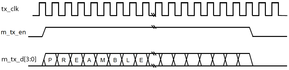
The parameter MBPS determines data rate of the transmit interface. If MBPS is set to 1, the TX speed in 100 Mbps; else if the MBPS is set to 0, the TX speed is 10 Mbps. The frequency of the TX clock is 25 Mhz in 100 Mbps mode and 2.5Mhz in 10Mbps mode. The IP core provides TX clock to MII MAC.
During transmission, the MII MAC asserts the m_tx_en signal and transmit 4-bit of data at each cycle of the TX clock. When there is an error in the transmission, the MII MAC asserts the m_tx_err signal synchronous to TX clock. The following figure shows a TX frame with m_tx_err.
Figure 161. TX Frame with Error Signal
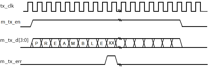
On detecting an TX error, the core transmits 01 pattern for the rest of the transmission over the output RMII interface, so that the frame fails the cyclic redundancy check (CRC).