MIPI D-PHY IP User Guide: Agilex™ 3 and Agilex™ 5 FPGAs
A newer version of this document is available. Customers should click here to go to the newest version.
7. MIPI D-PHY Architecture
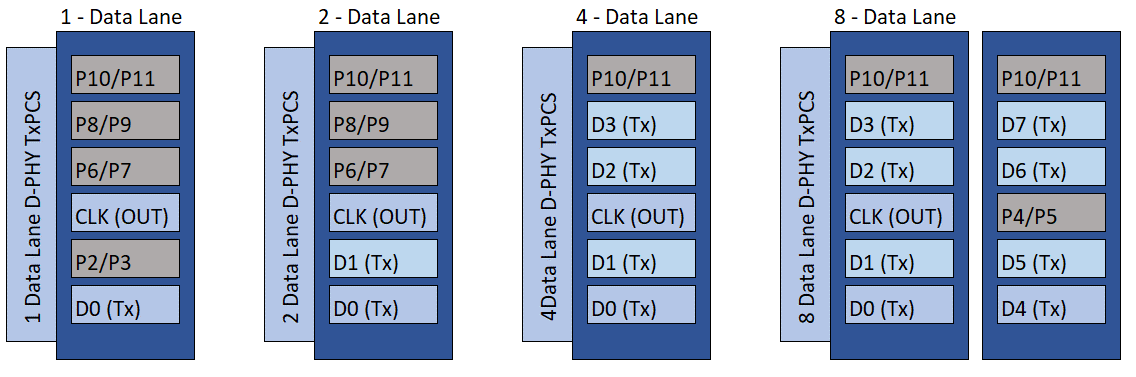
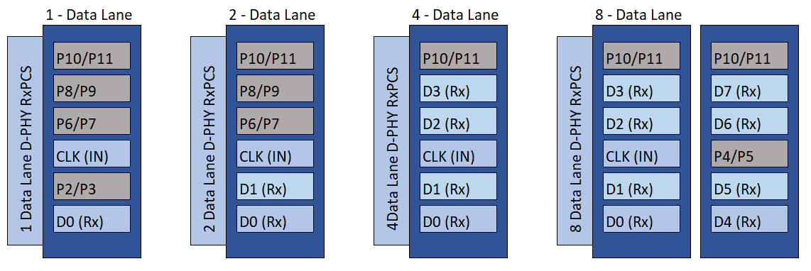
The Agilex™ 3 and Agilex™ 5 devices implement the MIPI D-PHY IP through HSIO banks. Each HSIO bank consists of 8 byte blocks to support MIPI D-PHY IP. However, one byte blocks is reserved for RZQ calibration and reference clock. Therefore the maximum MIPI D-PHY interfaces that a single HSIO bank can support is up to 7 interfaces (subject to D-PHY lanes configuration). Both the Agilex™ 3 and Agilex™ 5 devices offer a native D-PHY interface that allows direct point-to-point connection between the D-PHY transmitter and D-PHY receiver without any passive circuitry or third-party component in between. Each interface can support 1, 2, 4, or 8 data lanes plus 1 clock lane.