External Memory Interfaces Agilex™ 7 M-Series FPGA IP Design Example User Guide
ID
772632
Date
4/01/2024
Public
A newer version of this document is available. Customers should click here to go to the newest version.
1. About the External Memory Interfaces Agilex™ 7 M-Series FPGA IP
2. Design Example Quick Start Guide for External Memory Interfaces Agilex™ 7 M-Series FPGA IP
3. Design Example Description for External Memory Interfaces Agilex™ 7 M-Series FPGA IP
4. Document Revision History for External Memory Interfaces Agilex™ 7 M-Series FPGA IP Design Example User Guide
2.1. Creating an EMIF Project
2.2. Generating and Configuring the EMIF IP
2.3. Configuring DQ Pin Swizzling
2.4. Generating the Synthesizable EMIF Design Example
2.5. Generating the EMIF Design Example for Simulation
2.6. Pin Placement for Agilex™ 7 M-Series EMIF IP
2.7. Compiling the Agilex™ 7 M-Series EMIF Design Example
2.8. Using the EMIF Design Example with the Test Engine IP
2.9. Generating the EMIF Design Example with the Performance Monitor
2.1.1.3.1. Generating a Custom Memory Preset File for DDR4
2.1.1.3.2. Guidelines for Selecting the DDR4 DRAM Component Package Type
2.1.1.3.3. Generating a Custom Memory Preset File for DDR5
2.1.1.3.4. Guidelines for Selecting the DDR5 DRAM Component Package Type
2.1.1.3.5. Generating a Custom Memory Preset File for LPDDR5
2.3.1. Example: DQ Pin Swizzling Within DQS group for x32 DDR4 interface
2.3.2. Example: Byte Swizzling for a x32 DDR4 interface, using a memory device of x8 width
Example: Byte Swizzling for a x32 DDR4 interface, using a memory device of x8 width
2.3.3. Combining Pin and Byte Swizzling
2.3.4. Example: Swizzling for a x32 + ECC interface
2.3.5. Example: Byte Swizzling for Lockstep Configuration
2.3.2. Example: Byte Swizzling for a x32 DDR4 interface, using a memory device of x8 width
Example: Byte Swizzling for a x32 DDR4 interface, using a memory device of x8 width
| Lane Number | BL0 | BL1 | BL2 | BL3 | BL4 | BL5 | BL6 | BL7 |
|---|---|---|---|---|---|---|---|---|
| Default Placement | DQ[0] | AC[0] | AC[1] | AC[2] | DQ[1] | DQ[2] | DQ[3] | GPIO |
| After Byte Swizzling | DQ[2] | AC[0] | AC[1] | AC[2] | DQ[1] | DQ[0] | DQ[3] | GPIO |
| BYTE SWIZZLE | 2 | X | X | X | 1 | 0 | 3 | X |
This example illustrates swizzling DQS group 0 with DQS group 2. The BYTE_SWIZZLE_CH0 denotes the DQS group implemented in the lane after the swizzling. X indicates that the lane is not used as a data lane (meaning that it serves as an address/command lane or is not used by the EMIF interface).
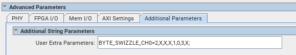
To achieve this swizzling, you must enter BYTE_SWIZZLE_CH0=2,X,X,X,1,0,3,X”; in the User Extra Parameters field of the Additional Parameters tab in the Advanced Parameters section of the General IP Parameters tab in the External Memory Interfaces IP parameter editor.
Figure 29. Swizzling DQS group 0 with DQS group 2