External Memory Interfaces Agilex™ 7 M-Series FPGA IP Design Example User Guide
A newer version of this document is available. Customers should click here to go to the newest version.
2.2.1. Agilex™ 7 M-Series EMIF Parameter Editor Guidelines
| Parameter Editor Tab | Guidelines |
|---|---|
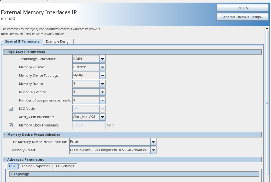
| High Level Parameters | Ensure that you correctly enter the following parameters:
|
| PHY | Select the desired mode to connect the EMIF IP to user logic:
|
| FPGA I/O and Mem I/O | Allows you to modify the termination and VREF settings. |
| Memory Device Preset Selection | Refer to the data sheet for your memory device and select the applicable preset. |
| AXI Settings | Set the AXI4 data width interface parameters according to your desired configuration. |
| Example Design | The Example Design tab lets you select which HDL to use for the top-level files, and which file sets you want the design example to generate. You should make these selections before clicking the Generate Example Design... button. The generated design example is a complete EMIF system consisting of the EMIF IP and a driver that generates random traffic to validate the memory interface. |
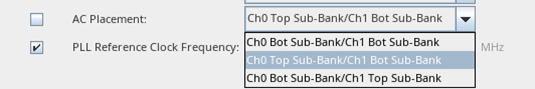
When using banks 2A and 2B, select Ch0 Bot Sub-Bank/Ch1 Bot Sub-Bank for the AC placement address and command placement parameter. For banks 3A/3B, 3C/3D, or 2C/2D, there are two options available for the AC placement parameter:
- You must select Ch0 Top Sub-Bank/Ch1 Bot Sub-Bank when placing CH0 address and command pins in the top sub-bank.
- You must select Ch0 Bot Sub-Bank/Ch1 Top Sub-Bank when placing CH0 address and command pins in the bottom sub-bank.
When using DIMMs with dual-die components, ensure that you select the appropriate Command-Address Mirroring value.

For additional information, refer to the DIMM Support subsection of the DDR5 Data Width Mapping topic in the External Memory Interfaces Agilex™ 7 M-Series FPGA IP User Guide.
For detailed information on individual parameters, refer to the appropriate protocol-specific chapter in the External Memory Interfaces Agilex™ 7 M-Series FPGA IP User Guide.