External Memory Interfaces Agilex™ 7 M-Series FPGA IP Design Example User Guide
ID
772632
Date
4/01/2024
Public
A newer version of this document is available. Customers should click here to go to the newest version.
1. About the External Memory Interfaces Agilex™ 7 M-Series FPGA IP
2. Design Example Quick Start Guide for External Memory Interfaces Agilex™ 7 M-Series FPGA IP
3. Design Example Description for External Memory Interfaces Agilex™ 7 M-Series FPGA IP
4. Document Revision History for External Memory Interfaces Agilex™ 7 M-Series FPGA IP Design Example User Guide
2.1. Creating an EMIF Project
2.2. Generating and Configuring the EMIF IP
2.3. Configuring DQ Pin Swizzling
2.4. Generating the Synthesizable EMIF Design Example
2.5. Generating the EMIF Design Example for Simulation
2.6. Pin Placement for Agilex™ 7 M-Series EMIF IP
2.7. Compiling the Agilex™ 7 M-Series EMIF Design Example
2.8. Using the EMIF Design Example with the Test Engine IP
2.9. Generating the EMIF Design Example with the Performance Monitor
2.1.1.3.1. Generating a Custom Memory Preset File for DDR4
2.1.1.3.2. Guidelines for Selecting the DDR4 DRAM Component Package Type
2.1.1.3.3. Generating a Custom Memory Preset File for DDR5
2.1.1.3.4. Guidelines for Selecting the DDR5 DRAM Component Package Type
2.1.1.3.5. Generating a Custom Memory Preset File for LPDDR5
2.3.1. Example: DQ Pin Swizzling Within DQS group for x32 DDR4 interface
2.3.2. Example: Byte Swizzling for a x32 DDR4 interface, using a memory device of x8 width
2.3.3. Combining Pin and Byte Swizzling
2.3.4. Example: Swizzling for a x32 + ECC interface
2.3.5. Example: Byte Swizzling for Lockstep Configuration
3.2. Simulation Design Example
The simulation design example contains the major blocks shown in the following figure.
- An instance of the synthesis design example. As described in the previous section, the synthesis design example contains a traffic generator and an instance of the memory interface.
- A memory model, which acts as a generic model that adheres to the memory protocol specifications. Frequently, memory vendors provide simulation models for their specific memory components that you can download from their websites.
Figure 40. Simulation Design Sync Fabric Mode
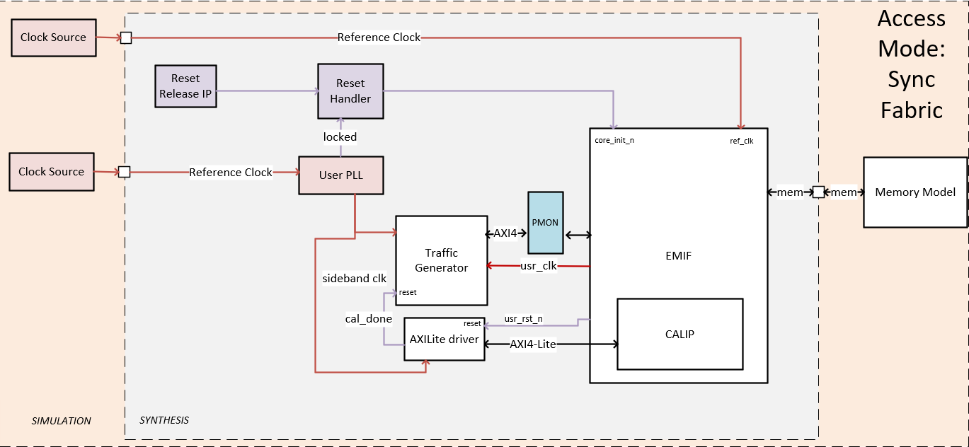
Figure 41. Simulation Design Async Fabric Mode
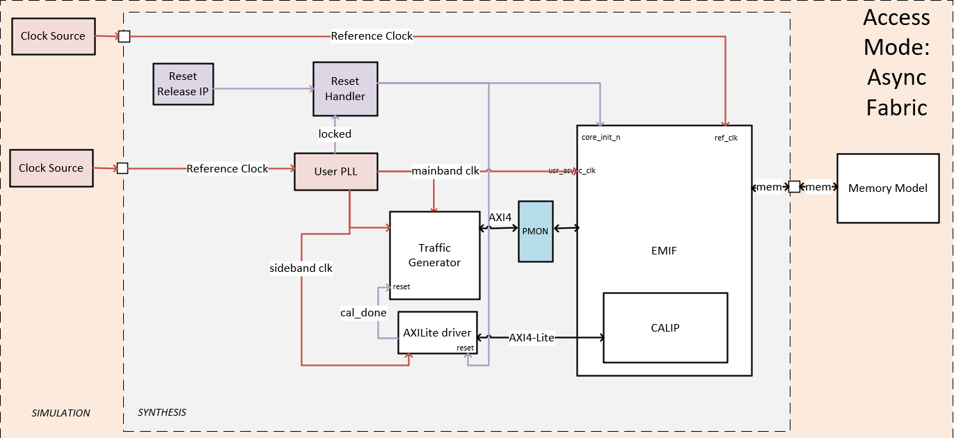
Figure 42. Simulation Design NOC Mode
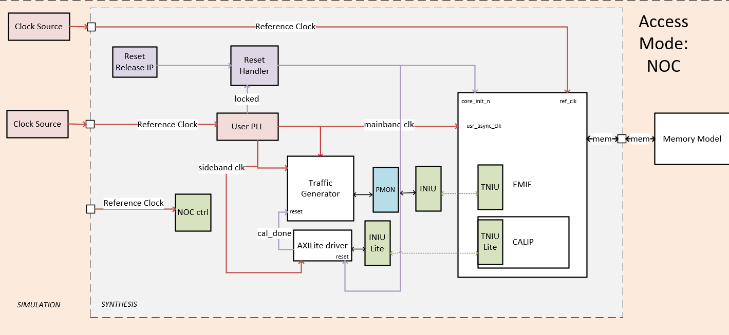
Note: You must place ref_clk_usr_pll. Refer to the Agilex™ 7 M-Series FPGA Network-on-Chip (NoC) User Guide for information on how to add NoC connectivity and address mapping to the simulation netlist.
If a user PLL shares an I/O bank with EMIF, you may additionally need to specify an operating voltage I/O standard. The voltage of the pin depends on the operating voltage of the EMIF occupying that bank, which, in turn, depends on the memory protocol, as follows:
- DDR4 = 1.2V
- DDR5 = 1.1V
- LPDDR5 = 0.7V
For example, for a PLL whose reference clock is in the same bank as a DDR5 EMIF, the assignment show look like this:
set_instance_assignment -name IO_STANDARD "1.1V True Differential Signaling" -to "ref_clk_usr_pll"