4. Agilex™ 7 FPGA Thermal Design Parameters
The Agilex™ 7 FPGA thermal parameters do not include the traditional junction-to-case thermal resistance (θJC) and junction-to-board thermal resistance (θJB) values, due to its multi-chip package construction. Instead of 2R resistor values, Altera provides a compact thermal model (CTM) of each package along with thermal parameters for each design through the Power and Thermal Calculator (PTC). The PTC thermal parameters include TJ, ΨCA, TAMBIENT, TCASE, ΨJC and total thermal power (TTP). The table below lists the thermal design parameters used in this document.
| Parameter | Description |
|---|---|
| TA | Ambient temperature, measured locally surrounding the FPGA. Measure the ambient temperature just upstream of a passive heat sink or at the fan inlet for an active heat sink. This value affects the junction temperature of the main FPGA core fabric die and its power dissipation. |
| TJ-MAX | The maximum rated junction temperature of a die, or could be the design goal. For example, a particular die could have a manufacturer's specified TJ-MAX of 100°C, but designers can specify a TJ-MAX of less than 100°C as part of their design requirement.
Note: The active junction temperature of the package TJ varies across the package and die, and varies with design. The junction temperatures across the package are used by the PTC only for more accurate power and temperature calculation.
|
| Power | The PTC reports the power dissipation of each die individually. |
| Total Thermal Power (TTP) | The total power dissipation of the device. This includes static power, with static power savings subtracted. The PTC reports this value in the Power Summary window. |
| ΨJC | The thermal resistance between each of the dies in the package and the center of the package integrated heat spreader. (See Figure 2). A multi-chip module (MCM) such as the Agilex™ 7 device will have as many ΨJC values as the number of dies in the package. The PTC reports the maximum ΨJC value which corresponds to the die with the highest temperature on the device. The ΨJC value is calculated by this equation:ΨJC = (TJ-MAX - TCASE) / TTP
Note: ΨJC values are not constant for a specific package and change as the FPGA resource usage changes.
|
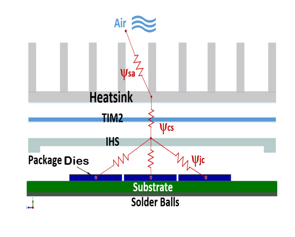
| ΨCA | The thermal resistance between the center of the package IHS and the ambient temperature. (See Figure 3.) ΨCA can be used as a figure of merit in assessing the required cooling solution for a design. For example, the lower the ΨCA value, the more aggressive cooling solution is needed. The value of ΨCA is calculated by this equation: ΨCA = (TCASE - TA) / TTP
Note: ΨCA values are not constant for a specific package and change as the FPGA resource usage changes. You must recalculate this value for each design.
|
| TCASE | The temperature at the top center of the IHS. For a design to not exceed its TJ-MAX, the cooling solution must be able to maintain the TCASE temperature at or below the TCASE temperature reported by the PTC.
Note: TCASE values are not constant for a specific package and change as the FPGA resource usage changes.
|
| Temperature Margin | Temperature margin is calculated relative to a designated maximum junction temperature, TJ. |
| Power Margin | Power margin indicates the power buffer available before the maximum junction temperature, TJ is exceeded. |
Figure 2. Individual Die Thermal Resistance to the Top of IHS
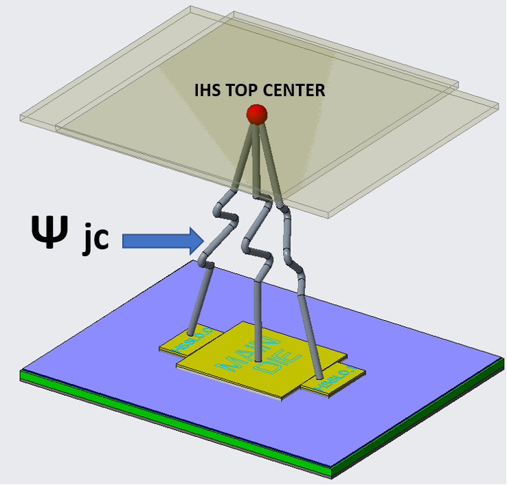
Figure 3. Thermal ResistanceThe diagram shows the thermal resistance from each die to the IHS top surface and also to the air.