Multi Channel DMA Intel® FPGA IP for PCI Express Design Example User Guide
A newer version of this document is available. Customers should click here to go to the newest version.
3.3.1. Testbench Overview
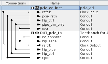
The testbench uses a Root Port driver module to initiate the configuration and exercise the target memory and DMA channel in the Endpoint. This is the module that you can modify to vary the transactions sent to the example Endpoint design or your own design.
- MCDMA R-Tile testbench
Path: pcie_ed_tb/ip/pcie_ed_tb/dut_pcie_tb_ip/intel_pcie_rtile_tbed_100/sim
File: altpcietb_bfm_rp_gen5_x16.sv
- MCDMA P-Tile testbench
Path: pcie_ed_tb/ip/pcie_ed_tb/DUT_pcie_tb_ip/intel_pcie_ptile_tbed_100/sim
File: altpcietb_bfm_rp_gen4_x16.sv
- MCDMA F-Tile testbench
Path: pcie_ed_tb/ip/pcie_ed_tb/dut_pcie_tb_ip/intel_pcie_ftile_tbed_100/sim
File: altpcietb_bfm_rp_gen4_x16.sv
- MCDMA H-Tile testbench
Path: pcie_ed_tb/ip/pcie_ed_tb/DUT_pcie_tb_ip/altera_pcie_s10_tbed_191/sim
File: altpcietb_bfm_rp_gen3_x8.sv