2.1.1. Constructing Communication Links in the Link Designer Module
2.1.2. Link and Simulation Setting
2.1.3. Transmitter Setting
2.1.4. Receiver Setting
2.1.5. IBIS-AMI Wrapper
2.1.6. Channel Setting
2.1.7. Batch Channel Simulation Configuration
2.1.8. Crosstalk Aggressor Transmitter Setting
2.1.9. Repeater and Retimer Configurations
2.1.10. Noise Source Link Component
2.1.11. System Options
2.1.12. Project Management Functions
2.1.13. Archiving and Unarchiving Projects
2.1.14. Device Model Importer
2.1.15. Analysis Functions and Pre-Simulation and Pre-Analysis Checklists
2.1.16. COM Analysis
2.1.17. Link Builder
3.2.1. Setting Up the Control Module
Link and Simulation Setting Tab
Figure 201. Link and Simulation Setting
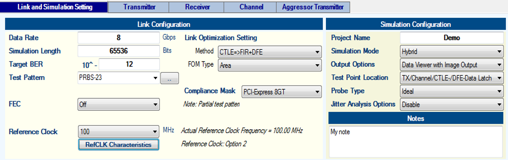
Set the following parameters in the Link and Simulation Setting tab:
- Data Rate: 8 (Gbps)
- Simulation Length: 65536 (Bits)
- Target BER: 10^ -12
- Test Pattern: PRBS-23
- Reference Clock: 100 (MHz)
- Link Optimization Method: CTLE=>FIR+DFE
- FOM of Link Optimization: Area
- Compliance Mask: PCI Express* 8GT
- FEC: Off. This disables forward error correction (FEC) modeling since the transmitter and receiver do not support FEC.
- Project Name: Demo
- Simulation Mode: Hybrid
- Output Options: Data Viewer with Image Output. This option tells Intel® Advanced Link Analyzer to generate image files (.png) for all output plots.
- Jitter Analysis Options: Disable. This selection disables the jitter analysis function during the link simulation.
Click Reference Clock Option.
Figure 202. Reference Clock Configuration
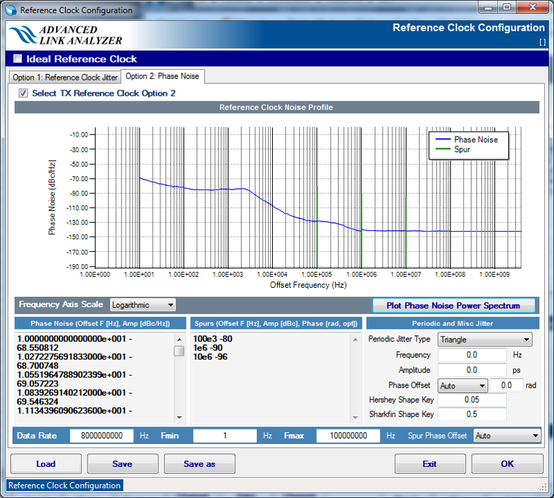
- Turn off the Ideal Reference Clock option
- Click the Option 2: Phase Noise tab
- Turn on the Select TX Reference Clock Option 2 option
- Type or copy the phase noise and spur data in the text boxes as shown in the above figure. The reference clock phase noise data can be found in the example configuration file Demo.jne.
Transmitter Tab
Figure 203. Transmitter Settings
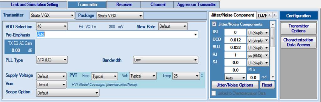
Set the following parameters in the Transmitter tab:
- Transmitter: Stratix® V GX
- Package: Stratix® V GX
- VOD Selection: 40 (~800 mV)
- Pre-emphasis: Auto
- PLL Type: ATX (LC)
- PLL Bandwidth: Low
- Jitter/Noise Component:
- If the Intel Device Characterization Data Access function is enabled, click Characterization Data Access. (A message box appears. Read and close the message box.) Transmitter jitter figures are populated automatically and the jitter/noise modeling mode is selected.
- If Intel Device Characterization Data Access is not available, manually type in the jitter numbers shown in the above figure. Note that the simulation results might differ slightly if the jitter data is from manual input.
Receiver Tab
Figure 204. Receiver Settings
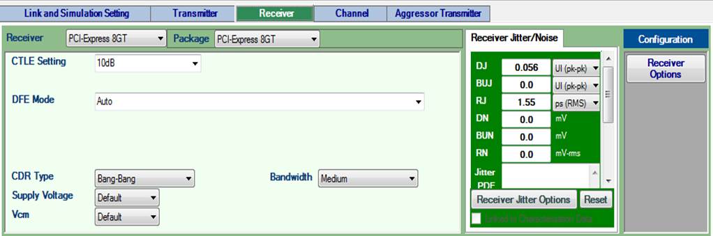
Set the following parameters in the Receiver tab:
- Receiver: PCI Express* 8GT
- Package: PCI Express* 8GT
- CTLE Setting: Auto
- DFE Mode: Auto
- CDR Type: Bang-Bang
- CDR Bandwidth: Medium
- PVT Process: Typical
- PVT Voltage: Typical
- PVT Temperature: 25 deg C
- DJ: 0.056 (UI, 7 ps)
- RJ: 1.55 ps (RMS) (key-in and then use pull-down menu to set RJ unit)
Note: In this simulation, the custom receiver is used to emulate a PCI-SIG PCI Express* 3.0 baseline receiver. The definitions of jitter components and values are different from that of PSG/Intel devices. Refer to compliance mask usage in the Link and Simulation Setting section for more details.
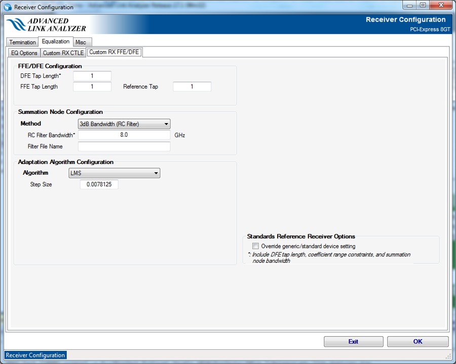
Click Receiver Options. In the Receiver Configuration window, click the Equalization tab. Set DFE Tap Length to 1 and Step Size to 0.0078125.
Figure 205. Additional Receiver Configuration
Related Information