2.1.2. Link and Simulation Setting
The Link and Simulation Setting tab sets the global link parameters and simulation configurations.
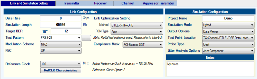
The Link and Simulation Setting dialog box contains the following fields:
Data Rate
The link data rate is specified in Gbps.
Simulation Length
The simulation length is specified in the number of bits running at the specified data rate. Simulation length should be at least 4096 bits. Intel® recommends that the length is a power-of-2 factor for the best computation efficiency. The simulation length does not apply in Statistical mode.
Target BER
Target bit error rate (BER) is used to calculate the jitter and noise at low BER conditions. If the simulation length exceeds the inverse of the target BER, the link performance is directly assessed and calculated. If the simulation length is shorter than the inverse of the specified target BER, Intel® Advanced Link Analyzer uses specific methodology and algorithms to calculate the link performance. The methodology of jitter and noise at low BER can be found in HST Jitter and BER Estimator Tool User Guide for Stratix® IV GT and GX Devices.
Test Pattern
Allows you to specify the test pattern used in the simulation. The following test patterns are available:
- PRBS-7, PRBS-9, PRBS-11, PRBS-15, PRBS-23, PRBS-31, and QPRBS13-CEI
- The PRBS test patterns are generated using Intel® Advanced Link Analyzer’s built-in pattern generator.
- If the PRBS pattern is shorter than the simulation length, the PRBS pattern is inverted and repeated. The inversion is applied to achieve the DC balance of the generated PRBS test pattern.
- If the PRBS patterns are longer than the simulation length, a partial test pattern of the PRBS pattern is used. The default initial condition of PRBS test pattern generation is with logic 1s in all shift registers for the valid PRBS patterns.
- The most commonly used PRBS test patterns are listed in the Test Pattern menu. Other PRBS test patterns can be selected or configured in the Pattern Designer.
-
Pattern Designer—Allows you to specify your custom test patterns. The following figure shows the Pattern Designer user interface:
Figure 6. Intel® Advanced Link Analyzer Pattern Designer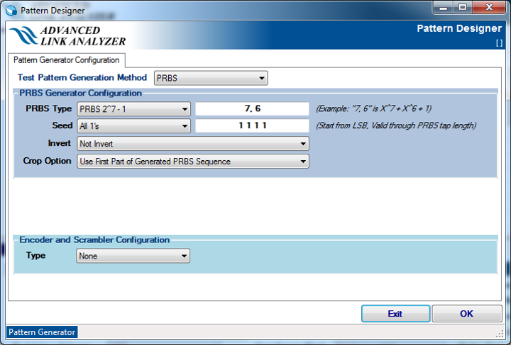
The Pattern Designer includes the following test pattern generation methods:
- PRBS—Provides an extensive list of common PRBS test patterns. You can also specify custom PRBS polynomials and seeds. The internal linear feedback shift register (LFSR) engine uses the information to generate the desired test pattern. Other options include selecting how the test pattern is repeated or extracted when the simulation length is longer or shorter than the generated test patterns. There are two options for selecting the partial test patterns:
- Use First Part of Generated PRBS Sequence
- Include Longest Run-Length Bit Sequence—The longest run-length test pattern is located at the ending portion of the test bit sequence.
- Consecutive Bit Patterns—Defines the test patterns with repeating patterns.
- Clock—Generates a clock-like pattern.
- All 1's—Generates an all-ones test pattern that usually feeds into a coder or scrambler.
- All 0's—Generates an all-zeros test pattern that usually feeds into a coder or scrambler.
- Encoder and Scrambler— Intel® Advanced Link Analyzer supports the following encoders and scramblers: 8B/10B, 64B/66B, 64B/67B, and 128B/130B.
- PRBS—Provides an extensive list of common PRBS test patterns. You can also specify custom PRBS polynomials and seeds. The internal linear feedback shift register (LFSR) engine uses the information to generate the desired test pattern. Other options include selecting how the test pattern is repeated or extracted when the simulation length is longer or shorter than the generated test patterns. There are two options for selecting the partial test patterns:
- Custom—Click the open-file dialog button to select a custom test pattern file.
Figure 7. Custom Test Pattern File Browser Button
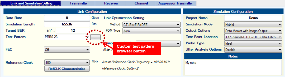
The custom pattern files are in the following formats:
- Hexadecimal—Hexadecimal strings start with 0x. For example, a PRBS-7 test pattern can be specified by 0x8cd501fbe7ae1ba62b05e3b64a4272d0. The custom file name must have a .hex extension.
- Binary—Binary strings have a format such as "001000111…". The input binary string file supports blank characters and new lines/returns. The custom file name must have a .bin extension.
Note: The custom test pattern has a maximum text length of 262,142 characters (about 1M bits with a hexadecimal text format or about 246K bits with a binary text format). Intel recommends that the test pattern string (hexadecimal or binary) is specified in a single row without spaces, especially for long custom test patterns. If a custom test pattern is input with multiple lines of text, the line returns or end-of-line control characters on each line of text are counted as an item or entry by the text parser.
Modulation Scheme
Intel® Advanced Link Analyzer supports NRZ and PAM4 modulation schemes. Choose PAM4 only when the device supports it.
Forward Error Correction (FEC)
FEC is a coding scheme that encodes the data pattern with additional code words to help the receiver to recover bit errors. Arria® 10, Stratix® 10, and Agilex™ 7 devices support FEC schemes. In Intel® Advanced Link Analyzer, the FireCode, Reed-Solomon RS (528, 514), RS (544, 514), RS (272, 258), and JESD204 FEC models are supported. When FEC is enabled, Intel® Advanced Link Analyzer produces additional FEC-related results. The default FEC setting is Off.
Reference Clock
You can specify the reference clock that feeds into the transmitter. The supported clock frequencies are shown in MHz. By default, the reference clock is assumed to be ideal without any noise or jitter. You can configure and specify the reference clock characteristics by clicking Reference Clock Option.
The reference clock can be fed to a transmitter with or without enabling a phase-locked loop (PLL) module. When the transmitter PLL is disabled or not present, the reference clock noise and jitter directly affect the serial output signal.
With integer PLLs, Intel® Advanced Link Analyzer supports an integer divider ratio between the data rate and the reference clock frequency. If the ratio is not an integer, the reference clock frequency is rounded to the closest integer-divided-ratio frequency. The actual reference clock frequency used in the simulation is displayed in the message box next to the pull-down menu. With fractional-N PLLs, fractional divider ratios are allowed.
In the simulation with specific transmitter devices, such as Arria® 10 GX/SX/GT, Stratix® V GT, Stratix® V GX, and Arria® V GZ devices, the supported data rate to reference clock divider ratios is limited. If a specific combination of data rate, PLL divider ratio, and reference clock frequency cannot be found, the reference clock used in the simulation can be further adjusted.
The reference clock frequencies listed are commonly used in most serial link protocols. If you cannot find the exact reference clock frequency from the list, you can add your reference clock frequency with the following procedure:
- Close Intel® Advanced Link Analyzer.
- Navigate to the Intel® Advanced Link Analyzer installation directory. Typically, Intel® Advanced Link Analyzer is installed in C:\intelFPGApro\<version number>\adv_link_analyzer\.
- Under the Database folder, find RefCLK_List.jnetxdata.
- Copy RefCLK_List.jnetxdata to your local directory (typically at C:\Users\<Your User or Account Name>\AdvancedLinkAnalyzer\<current version>\Database\.
- Edit the file by adding your desired reference clock frequencies.
- Save the change and exit the editor.
- Restart Intel® Advanced Link Analyzer.
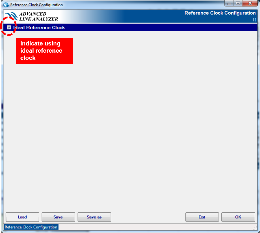
Reference Clock Option
The reference clock option user interface allows you to configure the characteristics of the reference clock used in the simulation. You can specify the reference clock with the following methods:
- Ideal Reference Clock—With this setting, the reference clock is ideal without any noise or jitter.
Figure 8. Ideal Reference Clock Setting
- Option 1: Reference Clock Jitter
Figure 9. Reference Clock Option 1: Reference Clock Jitter
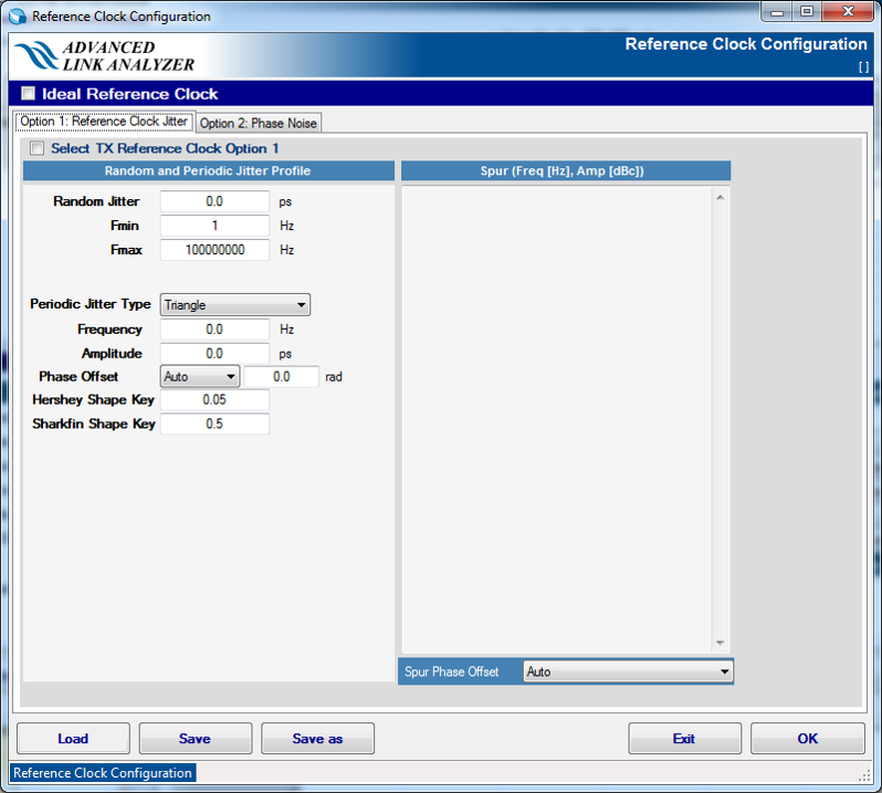
Option 1 configures the reference clock with the following options:
- Random Jitter— Specify the frequency range (in ps).
Note: Intel recommends that the maximum frequency range (fMAX) of the phase noise be set to the reference clock frequency. If the fMAX is less than the reference clock frequency, Intel® Advanced Link Analyzer uses linear extrapolation to calculate the phase noise at fMAX, which can lead to inaccurate results.
- Periodic Jitter Type—Specify the shape profile, frequency (Hz), and amplitude (ps). The shape profile can be:
- Triangle
- Hershey with programmable Hershey shape parameter
- Sharkfin with programmable Sharkfin shape parameter
- Sinusoidal
- Spurs—Specify clock spectrum spurs with individual frequency (in Hz) and amplitude (dBc). For example, if the reference clock has three spurs: –110 dBc at 100 kHz, –90 dBc at 1 MHz, and –80 dBc at 10 MHz, you can input the following text into the Spurs text box:
100e3 -110
1e6 -90
10e6 -80
- Spur Phase Offset
Use the Spur Phase Offset pull-down menu to configure the initial phase of spur noises. The options are:
- Auto— Intel® Advanced Link Analyzer automatically selects the default initial spur noise phase. The default initial spur phase is 0 rad.
- Random— Intel® Advanced Link Analyzer randomly sets the initial spur noise phases.
- Zero— Intel® Advanced Link Analyzer sets the initial spur noise phase to 0 rad.
- Specified—You can manually specify the initial spur phase individually by adding the phase value after the amplitude value. The following example shows the initial spur noise phases are 1.0, 2.0, and 3.0 rad.
100e3 -110 1.0
1e6 -90 2.0
10e6 -80 3.0
- Option 2: Phase Noise
Figure 10. Reference Clock Option 2: Phase Noise
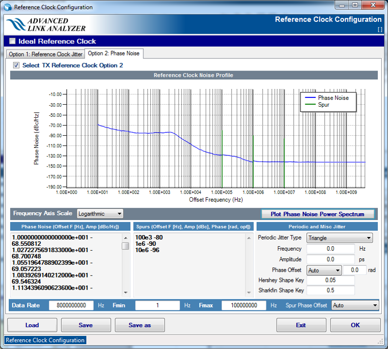
Option 2 configures the reference clock with the following options:
- Phase Noise—Specify reference clock jitter using a phase noise profile. Reference clock phase noise is specified with the noise power spectrum described with frequency and amplitude. The above figure demonstrates a phase noise profile with a measured reference clock phase noise data set.
Note: Intel recommends that the maximum frequency range (fMAX) of the phase noise be set to the reference clock frequency. If the fMAX is less than the reference clock frequency, Intel® Advanced Link Analyzer uses linear extrapolation to calculate the phase noise at fMAX, which can lead to inaccurate results.
- Spurs—Specify clock spectrum spurs with individual frequency (in Hz) and amplitude (in dBc). For example, if the reference clock has three spurs: –80 dBc at 100 kHz, –90 dBc at 1 MHz, and –96 dBc at 10 MHz, you can input the following text into the text box:
100e3 -80
1e6 -90
10e6 -96
- Spur Phase Offset—Same as in Option 1 Reference Clock Jitter.
- Periodic Jitter Type—Same as in Option 1 Reference Clock Jitter.
- Plot / Update Plot—You can plot the input phase noise and spurs in the plotting area and confirm the reference clock characteristics.
Link Optimization Method
Intel® Advanced Link Analyzer can find optimal transmitter and receiver equalization settings with a user-specified link configuration.
| Transmitter Mode |
Receiver Mode |
Notes |
|---|---|---|
| Manual |
Manual |
Both TX and RX equalizations are manually set. |
| Auto / Auto with Manual Starting Point |
Manual |
Intel® Advanced Link Analyzer finds optimal TX equalization setting. RX EQ setting is manually set. |
| Manual |
Auto |
TX EQ is manually set. Intel® Advanced Link Analyzer finds optimal RX EQ setting. |
| Auto / Auto with Manual Starting Point |
Auto |
Intel® Advanced Link Analyzer finds both TX and RX EQ settings. |
Intel® Advanced Link Analyzer has four link optimization methods for finding the optimal link setting, such as a transmitter pre-emphasis and receiver CTLE and DFE with a given link configuration.
- FIR=>CTLE=>DFE— (default) Optimizes the link performance by finding the optimal transmitter setting, receiver equalization setting, or both. This method prioritizes the transmitter equalization, such as pre-emphasis, de-emphasis, or FIR-based, over receiver equalization schemes. However, the optimization algorithm can also capable detect and utilize optimal receiver equalization. In practice, this usually implies the transmitter equalization performs most of the "heavy-lifting" in channel compensation.
- FIR=>CTLE+DFE—Extends the FIR=>CTLE=>DFE method by enabling RX DFE (Decision Feedback Equalizer) when RX optimization is performed. This method exploits DFE capabilities by possibly reducing the channel compensation from CTLE (depending on the channel characteristics).
- CTLE=>FIR=>DFE—Prioritizes the receiver's CTLE capability over the transmitter's equalization. Most of the channel compensation is performed by the receiver's CTLE, while the TX equalization provides additional compensation if needed. RX DFE is adopted in the final stage. This method is supported in non-IBIS-AMI devices. For Intel transmitters, you can manually set initial TX FIR configurations so the link optimizations can yield better solutions with shorter simulation time when the initial conditions are proper.
- CTLE=>FIR+DFE—Extends the CTLE= FIR=>DFE method by joint-optimizing TX pre-emphasis/FIR and RX DFE. This method allows co-optimization between the TX FIR and RX DFE. For Intel transmitters, you can manually set the initial TX FIR configurations so the link optimizations can yield better solutions more quickly when the initial conditions are proper.
- CTLE=>FIR=>CTLE=>DFE—Extends the CTLE=>FIR=>DFE method by performing an additional CTLE adaptation stage after the FIR setting is found.
- CTLE=>FIR+DFE=>CTLE+DFE—Extends the CTLE=>FIR+DFE method by performing an additional CTLE+DFE adaptation stage.
- ALA-COM—COM (Channel Operating Margin) based joint link optimization method. This is a beta feature in 24.1 that supports Custom and Agilex™ 7 transceiver models only.
Use the following guidelines for choosing the best link optimization method:
- FIR=>CTLE=>DFE is a good choice for most applications or channels for time-efficient link optimizations. It is the default link optimization method in Intel® Advanced Link Analyzer.
- For heavy insertion loss channels, such as when insertion loss > 25 dB at Nyquist frequency, FIR=>CTLE=>DFE provides good coverage.
- For strong impedance discontinuities, CTLE=>FIR=>DFE and CTLE=>FIR=> CTLE=>DFE methods provide better performance in general.
- For large crosstalk noises, choose FIR=>CTLE+DFE for high loss channels or CTLE=>FIR+DFE and CTLE=>FIR+DFE=>CTLE+DFE for moderate loss applications.
Notes:
- Intel® Advanced Link Analyzer supports link optimization for selected IBIS-AMI models for the link optimization modes and the methods shown above. Refer to the IBIS-AMI model support sections for details.
- For a transmitter equalization sweep simulation, Intel® Advanced Link Analyzer provides batch simulation capability using the Intel® Advanced Link Analyzer Batch Simulation Controller tool. Refer to the Intel® Advanced Link Analyzer Batch Simulation Controller section for details.
FOM of Link Optimization
Use this menu to select the figure of merit (FOM) for optimizing the serial link. There are three options: Area, Width, and Height. The signal conditioning mechanisms, which include transmitter pre-emphasis, de-emphasis, and receiver equalizers, use these selections to optimize the waveform so that it has the best eye diagram opening in terms of area, width, or height.
Compliance Mask
Intel® Advanced Link Analyzer plots link compliance eye diagram masks after completing the simulations. Use a compliance mask to examine whether the waveform or eye diagram meets the receiver's requirements at certain conditions (such as BER target). PCI Express* 8GT/16GT and selected devices’ receiver eye masks are provided.
Eye Diagram Mask Designer
Intel® Advanced Link Analyzer supports custom eye diagram mask definitions at various locations within a link. When the Eye Diagram Mask Designer option is selected, the custom eye diagram mask configuration window opens. You can then specify the dimension of the eye diagram mask. The custom eye diagram mask is used in the simulation. Two eye diagram mask types are supported. Four different eye diagram masks can be specified for transmitter output, channel output, receiver CTLE output, and link/receiver output. Each eye diagram mask can be individually configured and enabled.
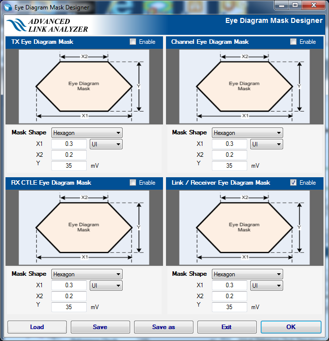
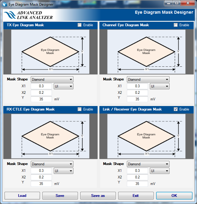
A custom eye diagram mask can be saved and loaded for future use.
Project Name
Project Name is a user-defined name for the current task/project. Currently, the session name is the saved user configuration file name when the simulation configuration is saved.
Notes:
- The simulation results are automatically written to a directory with the same project name.
- The location of the output directory can be configured as one of the following:
- The same location as the project configuration file (.jne/.jneschm) (this is the default).
- A location you specify in the System options. Refer to the System Options section for details.
- Intel® recommends that there should be no space (or bland) characters in the project name.
Simulation Mode
Intel® Advanced Link Analyzer provides three simulation modes (statistical, full waveform, and hybrid) to meet your simulation and link analysis preferences and needs. Hybrid mode is the default.
| Statistical Mode |
Full Waveform Mode |
Hybrid Mode (Default) |
|
|---|---|---|---|
| Simulation Method |
Statistical Method |
Time-domain Method |
Time-domain and Statistical Methods |
| Jitter Injection and Simulation |
Statistical Domain (PDF-based) |
Time Domain |
Mixed Domain (Time Domain and PDF-based) |
| Noise Injection and Simulation |
Statistical Domain (PDF-based) |
Time Domain |
Mixed Domain (Time Domain and PDF-based) |
| Simulation Speed (to meet your specified BER target) |
Fast |
Slow |
Optimal |
| Accuracy |
Lower |
Best |
Optimal |
| Recommended Simulation Length |
N/A (You do not need to specify simulation length in statistical mode.) |
>1,000,000 bits |
60,000-1,000,000 bits |
Further information and comparisons among the three simulation modes can be found in the following papers:
- Comparison of Two Statistical Methods for High-Speed Serial Link Simulation by M. Shimanouchi, M. Li, and H. Wu. DesignCon, 2013, Santa Clara, CA.
- Advancements in High-Speed Link Modeling and Simulation by M. Li, M. Shimanouchi, and H. Wu. IEEE Custom Integrated Circuits Conference, 2013.
- High-Speed Link Simulation Strategy for Meeting Ultra Long Data Pattern under Low BER Requirements by H. Wu, M. Shimanouchi, and M. Li, DesignCon, 2014, Santa Clara, CA.
Output Options
- Data Viewer—When the simulation is complete, a new Intel® Advanced Link Analyzer Data Viewer opens and the results are shown. The simulation results can be loaded and viewed later with Intel® Advanced Link Analyzer Data Viewer.
- Data Viewer with Image Output—When the simulation is complete, all the simulation results are also saved as image files that can be used in documentation. Intel® Advanced Link Analyzer supports three image output options: PNG, JPEG, and GIF. The saved images are located in the same directory as the simulation results for each project.
Test Point Options
Intel® Advanced Link Analyzer provides the following default test point options:
- Data Latch Only—Simulation results at the data latch are saved and displayed. Data latch can be at DFE output, CTLE output, or the input stage of the receiver depending on the link or device configuration. Custom test points and simulation results at test points are not shown.
Note: For simulation length longer than 1 million bits, it is suggested to use Data Latch Only mode to reduce overall simulation time.
- TX/Channel/CTLE-/DFE-Latch— Intel® Advanced Link Analyzer automatically sets up to four test points for the link:
- Transmitter output—(default option) If a transmitter package model is present (for example, the package model is embedded, as in Intel devices and PCI Express* 8GT) or external (for example, using the "Custom" package option), the output appears after the package model. If no package model is present, the output appears at the transmitter output.
- Channel output—The second test point is at the end of channels.
- CTLE output—If you enable the receiver CTLE, the third test point is at the output of the CTLE.
- DFE output—The fourth test point is at the output of the receiver DFE.
Note: Custom test points are neglected with this test point option. - Custom Test Point and Data Latch— Intel® Advanced Link Analyzer plots the output at custom test points and the final data latch point.
Probe Type
Intel® Advanced Link Analyzer provides two types of probes:
- Ideal—With an ideal probe, the waveform, signal, or eye diagram is plotted by assuming that the link is terminated with an ideal 50 ohms termination at the probe location.
- High-Impedance—With a high-impedance probe, the waveform, signal, or eye diagram is plotted by emulating a high-impedance probe sensing the probe location.
Jitter Analysis Options
Intel® Advanced Link Analyzer can perform jitter decomposition and links analysis for using NRZ modulation scheme on a waveform at specified test points. For PAM4 links, jitter analysis is performed using PAM4 Jnu/Jrms/EOJ method. See Jnu/Jrms/EOJ Analysis for details.
- Disable—Jitter analysis is disabled.
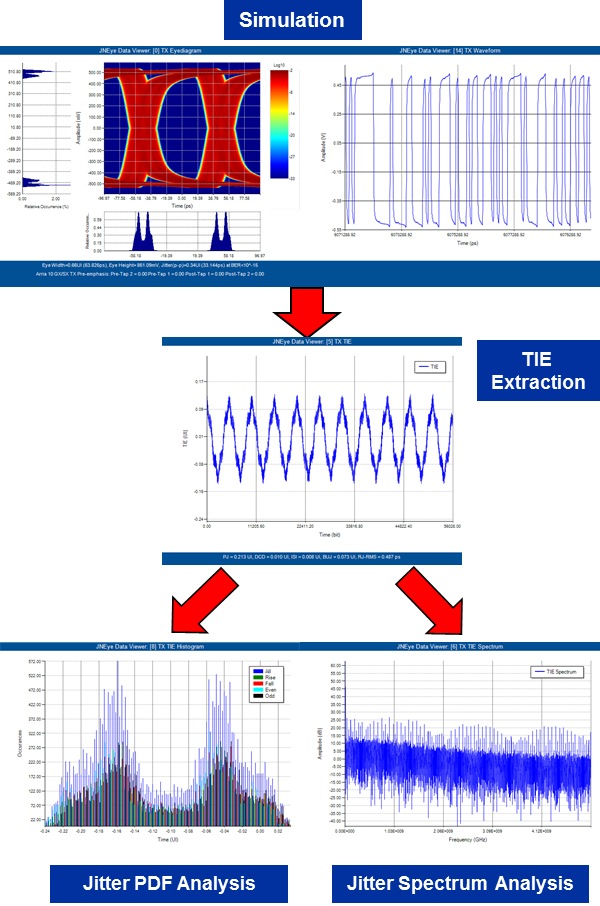
- Jitter Component—Using proprietary algorithms, Intel® Advanced Link Analyzer performs a series of spectrum and probability density function (PDF) analyses on the time-interval-error (TIE) record of the simulated waveforms. The jitter decomposition algorithms extract various jitter components, as shown in the following figure:
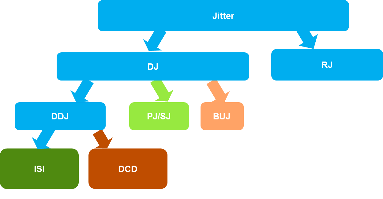
The jitter decomposition process (conceptual) is shown in the following figure:
The following jitter components are extracted and reported:
- PJ—Periodic jitter (peak-peak)
- DCD—Duty cycle distortion (peak-peak)
- ISI—Inter-symbol interference (peak-peak)
- BUJ—Bounded uncorrelated jitter (peak-peak)
- RJ-RMS—Random jitter (RMS)
- Jitter analysis is available in Hybrid simulation mode only. Currently, jitter decomposition supports the NRZ modulation scheme only.
- Jitter analysis is a time-consuming process. Intel recommends disabling this feature for general link simulations.