3.3. Analysis
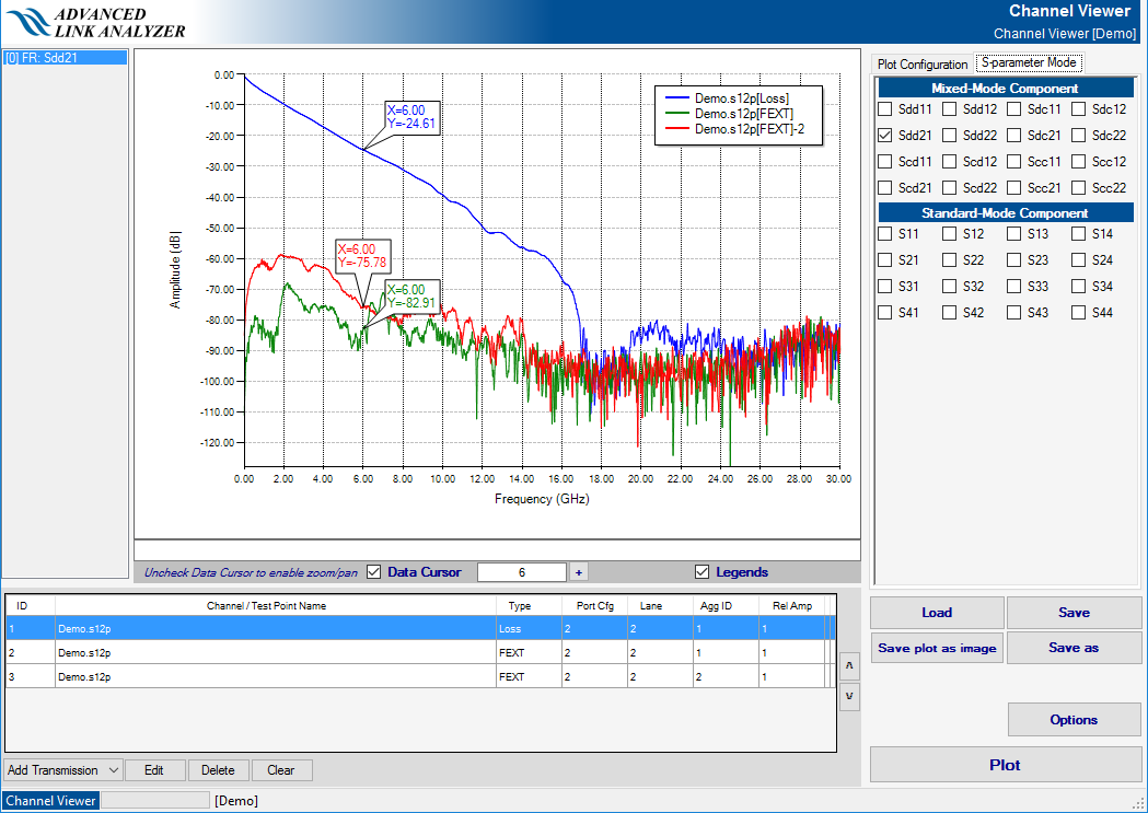
Use the Channel Viewer to observe and analyze the channel characteristics. The Channel Viewer button is located on the right side of the Channel tab. This example shows the Sdd21 of the three channels you selected as well as the channel responses at test points and the overall channel. You can leave the Channel Viewer module open or close it by clicking OK or Exit.
Start the channel simulation by clicking Simulate in the lower right corner of the Intel® Advanced Link Analyzer Control Module. The Intel® Advanced Link Analyzer Simulation Engine simulates all the models and generates eye diagrams at test points and inside the receiver (after CTLE and DFE).
A goal of this tutorial was for Intel® Advanced Link Analyzer to automatically find the optimal link setting for both transmitter and receiver. In the simulation time, the progress bar flashes, indicating the Intel® Advanced Link Analyzer Simulation Engine is exploring the solution space. The link performance and result of the final setting is shown in a Intel® Advanced Link Analyzer Data View.
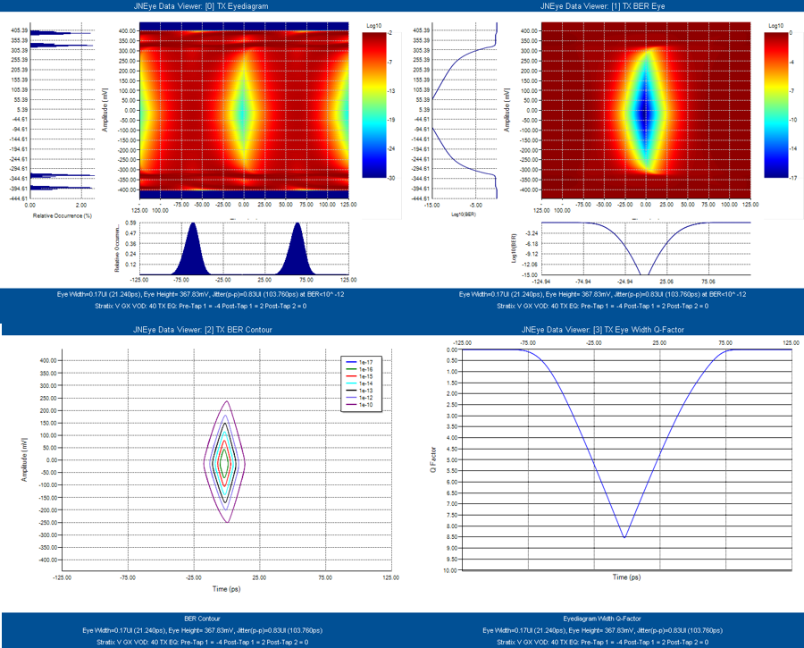
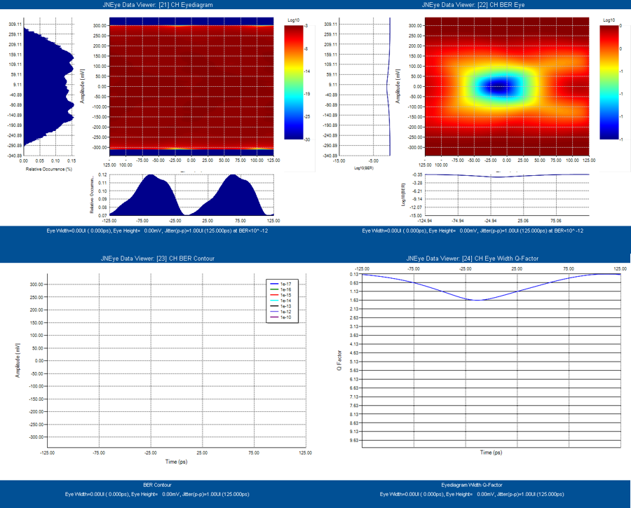
At TX output, which is located after the Intel Stratix® V GX transmitter output pin (after the TX package model), the results are shown in the following figure. Intel® Advanced Link Analyzer found the optimal TX-FIR setting: Pre-tap 1 = –4, Post-tap 1 = 2, and Post-tap 2 = 0. The configured transmitter generates ~0.83 UI of jitter at BER = 10-12. This set of TX outputs is measured with an ideal clock. In addition to the transmitter’s intrinsic jitter, the reference clock’s jitter and noise (recall that external reference clock phase noise and spurs in this simulation are filtered by the Stratix® V GX ’s PLL) are seen here.
- The first figure is a hybrid eye diagram that includes deterministic jitter and probability density function (PDF) because of unbounded jitter and noise sources.
- The second figure (top right) contains the cumulative distribution (CDF) eye diagram with BER bathtub curves (for both width and height in the eye diagram opening).
- The third plot (lower left) is a BER contour plot that shows the eye diagram opening area at various BER targets.
- The fourth plot shows Q-Factor curves, which are another representation of BER bathtub curve using Q-factor by assuming the noise/jitter is Gaussian.
With the Gaussian random jitter injected into the link, the BER bathtub and Q-Factor plots clearly show the effects where this unbounded jitter narrows the eye diagram width as the BER target reduces.
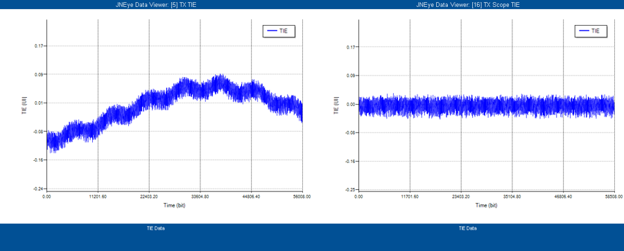
The second set of TX outputs are measured with the golden CDR, which has a loop bandwidth of 1/1667 of the data rate. This set of outputs reflects the common lab scope measurement. With the golden CDR in place, the low frequency jitter and noise, which are included in phase noise and spurs, are tracked.
The following figure shows the Time Interval Error (TIE) plots before and after the golden CDR. With reference to the ideal clock (that is, before the golden CDR), the low frequency sinusoidal jitter from the reference clock characteristics can be clearly observed in the plot on the left. After the golden CDR, those low frequency sinusoidal jitters are tracked as shown in the plot on the right. The figure also shows the jitter components results that reflect the effects of the golden CDR (Beta feature).
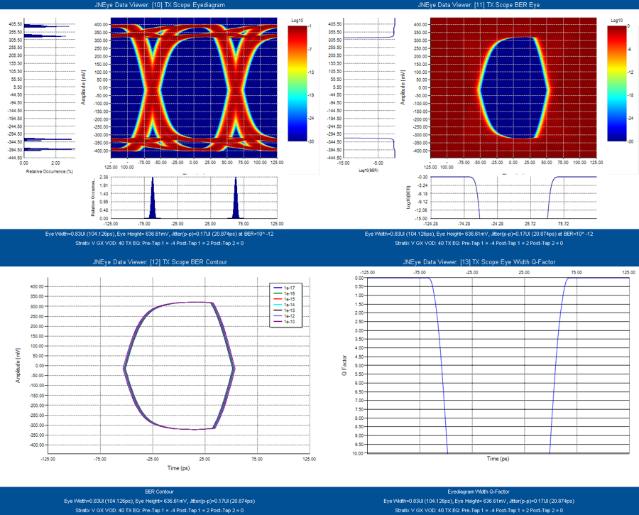
In the following figure, the transmitter output jitter, which includes transmitter intrinsic jitter and PLL filtered reference clock jitter, is about 0.17 UI at BER 10-12.
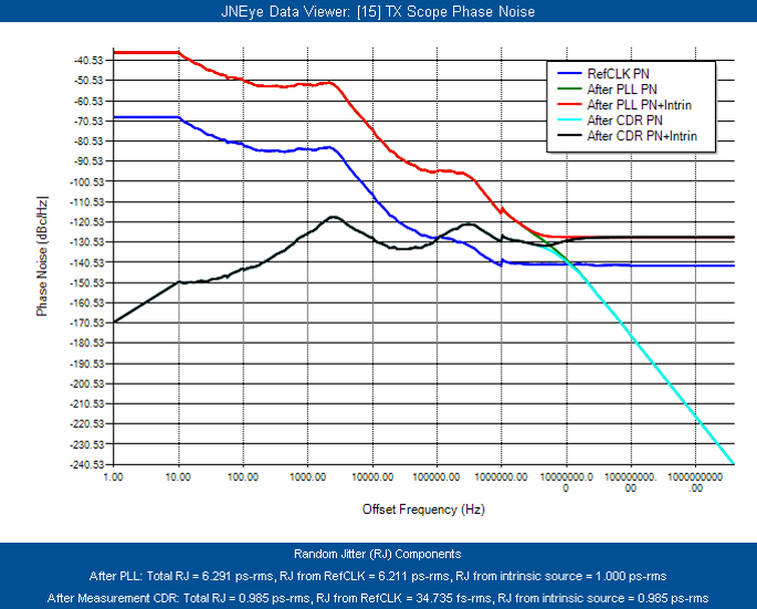
When you enable a PLL in a transmitter, the reference clock’s phase noise is shaped and filtered with the PLL’s response. The following figure shows the characteristics of phase noise at the output of the reference clock (blue), after the transmitter PLL (green), after the transmitter PLL plus the transmitter’s intrinsic jitter (red), after the Golden CDR (most likely in a scope, cyan), and after the Golden CDR with transmitter’s intrinsic jitter (black). The associated random jitter from the phase noise power spectrum at each of the above stages are calculated and displayed in the text below the plot.
At the channel output, which is located at the end of backplane channel with crosstalk, the eye diagram is largely closed because of the large channel loss from the TX package and the backplane.
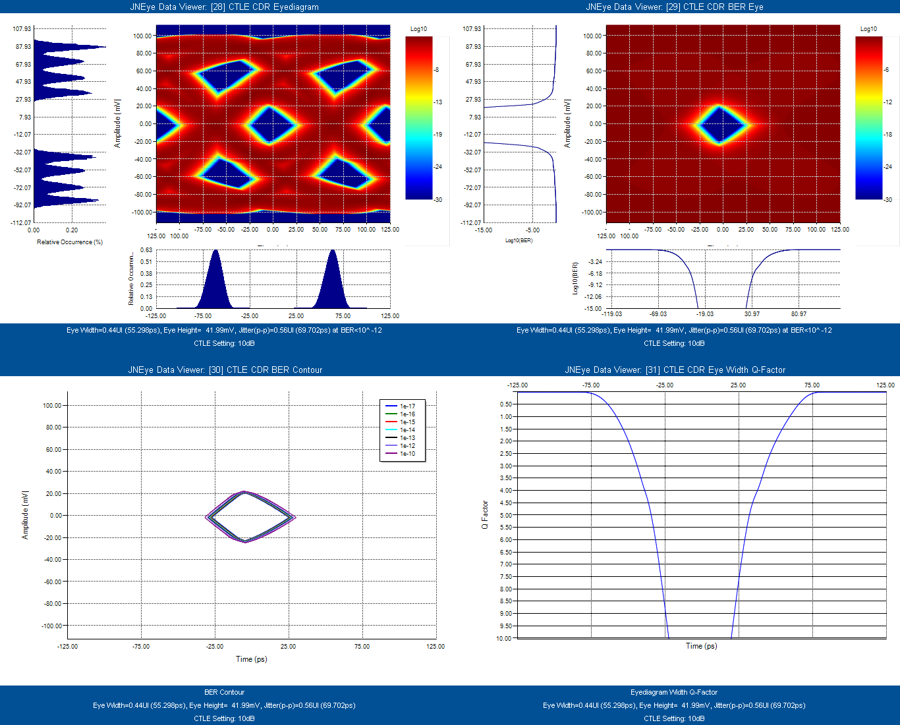
The CTLE is a PCI Express* 8GT CTLE behavior model output stage. The Intel® Advanced Link Analyzer's link optimization algorithm has identified the optimal gain setting at 10 dB level. Similar to the TX output case, when the receiver CDR is enabled or included in the simulation, two sets of CTLE outputs can be shown but, by default, Intel® Advanced Link Analyzer only outputs CDR retimed output when the receiver CDR is enabled. The first set of outputs is with the ideal clock and the second one is with the CDR recovered clock. The total jitter is ~0.94 UI (at BER < 10-12, with ideal clock, result not shown by default because receiver CDR is enabled) or ~0.56 UI (with CDR recovered clock). The eye diagram opening height is ~7 mV (with ideal clock, result not shown by default because receiver CDR is enabled) and ~42 mV (with recovered clock). The eye diagram opening is marginal to PCI Express* 8GT requirements. Therefore, further equalization of the signal with DFE is needed.
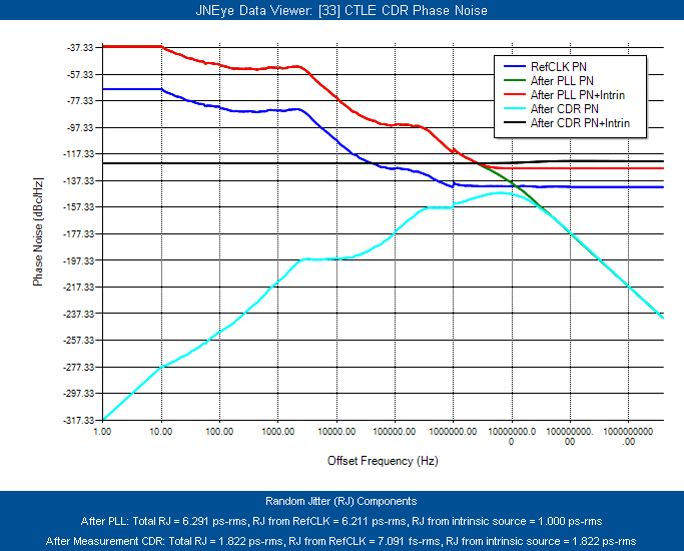
When you enable CDR in a receiver, the reference clock’s phase noise is shaped and filtered with the CDR’s response. The following figure shows the characteristics of phase noise at the output of the reference clock (blue), after the transmitter PLL (red), after the transmitter PLL plus the transmitter’s intrinsic jitter (red), after the RX CDR (cyan), and after the RX CDR with transmitter and receiver’s intrinsic jitter (black). The associated random jitter from the phase noise power spectrum at each of the above stages was calculated and displayed in the text below the plot.

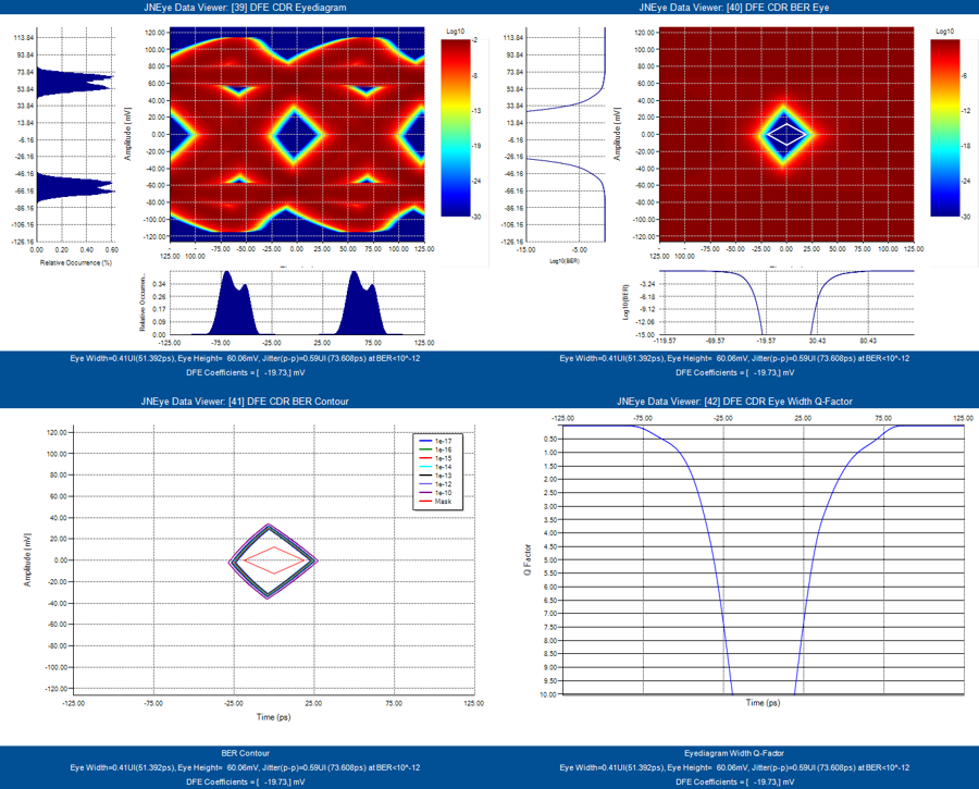
At the output of the PCI Express* 8G receiver’s 1-Tap DFE, the following figures show that the DFE has further opened the eye diagram with a total jitter of ~0.96 UI (at BER < 10-12, with ideal clock and sinusoidal jitter from the transmitter reference clock, result not shown by default because receiver CDR is enabled) and ~0.59 UI (with CDR recovered clock) and eye diagram opening height of ~3 mV (with ideal clock, result not shown by default because receiver CDR is enabled) and ~60 mV (with recovered clock). The BER bathtub curve and contour show good behavior and successfully meet the PCI Express* 8GT RX requirements (TJ < 0.7 UI and eye diagram height > 25 mV; refer to PCI Express* Base Specification 4.3).
The PCI Express* 8GT eye diagram mask is shown in the following figure to see the margins to the specification limits.
When you enable a CDR in a receiver, the reference clock’s phase noise is shaped and filtered with the CDR’s response. The following figure shows the characteristics of phase noise at the output of the reference clock (blue), after transmitter PLL (red), after transmitter PLL plus transmitter’s intrinsic jitter (red), after RX CDR (cyan), and after RX CDR with transmitter and receiver’s intrinsic jitter (black). The associated random jitter from the phase noise power spectrum at each of the above stages are calculated and displayed in the text below the plot.
These examples demonstrated how to use Intel® Advanced Link Analyzer to set up a serial link and evaluate its link performance. Intel® Advanced Link Analyzer allows you to:
- Configure a link
- Configure an external reference clock
- Configure a transmitter and receiver
- Configure a channel
- Configure and model jitter and noise sources
- Derive accurate jitter figures for Intel devices from the Intel JBE database
- Load and save a link configuration
- Observe the channel characteristics
- Set up test points within the link
- Compute and observe an eye diagram
- Perform BER analysis