1.6.1. Simulation Results for Stratix V GT to CFP2 Connector Layout Design
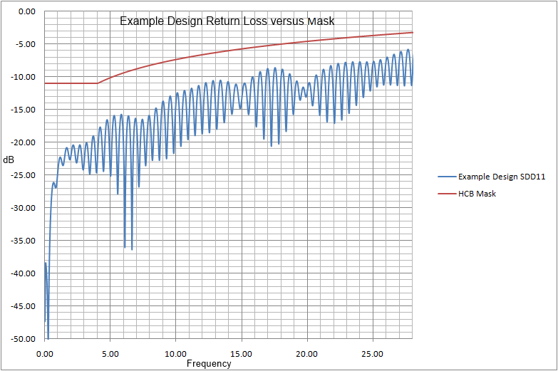
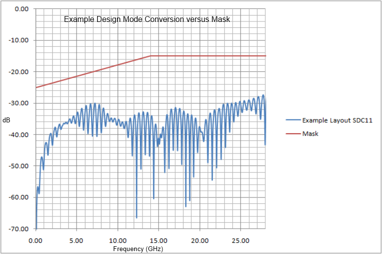
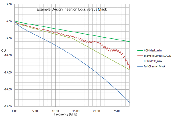
Ansys HFSS (High Frequency Structural Simulator) simulation results for the insertion loss (SDD21), return loss (SDD11) and differential-to-common mode conversion (SDC11) of the channel with the CFP2 connector included are shown in the following figures. The simulation models the HCB for validating the channel layout against the CEI-28G-VSR defined masks.
The SDD21 resides within the HCB minimum and maximum insertion loss masks as defined by the CEI-28G-VSR specification. This insertion loss meets the complete VSR channel (host board + connector + optical module) mask requirement with ample margin to accommodate the additional loss of an inserted CFP2 optical module. Note that the complete channel with the optical module is not simulated.
Similarly, the figures below show that the return loss and differential-to-common mode conversion both meet their respective masks as defined by the CEI-28G-VSR requirement.