External Memory Interfaces Intel® Agilex™ FPGA IP User Guide
A newer version of this document is available. Customers should click here to go to the newest version.
3.1.3. Intel® Agilex™ EMIF Architecture: I/O Bank
Each I/O bank consists of two sub-banks, and each sub-bank contains the following components:
- Hard memory controller
- Sequencer components
- I/O PLL and PHY clock trees
- DLL
- Input DQS clock trees
- 48 pins, organized into four I/O lanes of 12 pins each
A single I/O sub-bank contains all the hardware needed to build an external memory interface. You can make a wider interface by connecting multiple adjacent sub-banks together.
Within an I/O bank, the top sub-bank is placed near the edge of the die, and the bottom sub-bank is placed near the FPGA core.
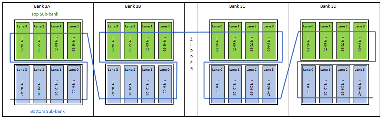
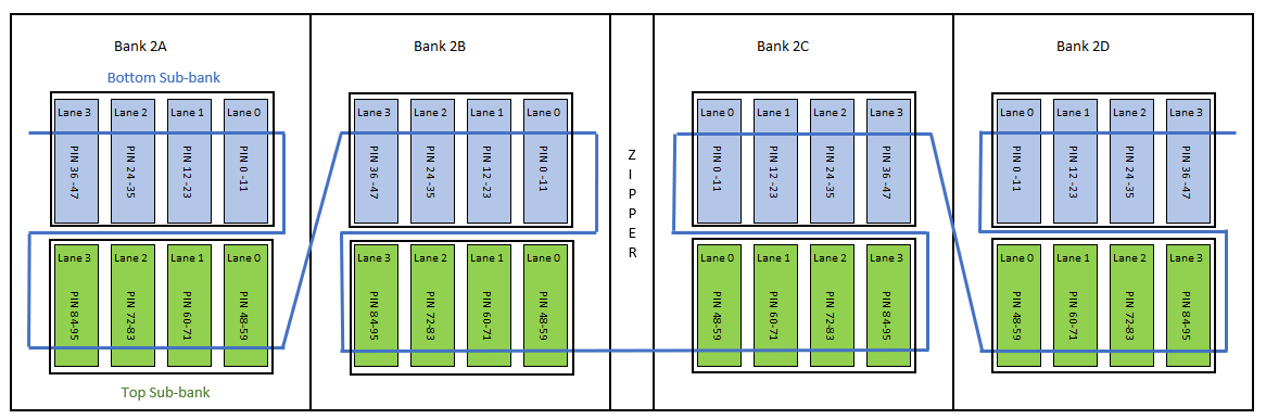
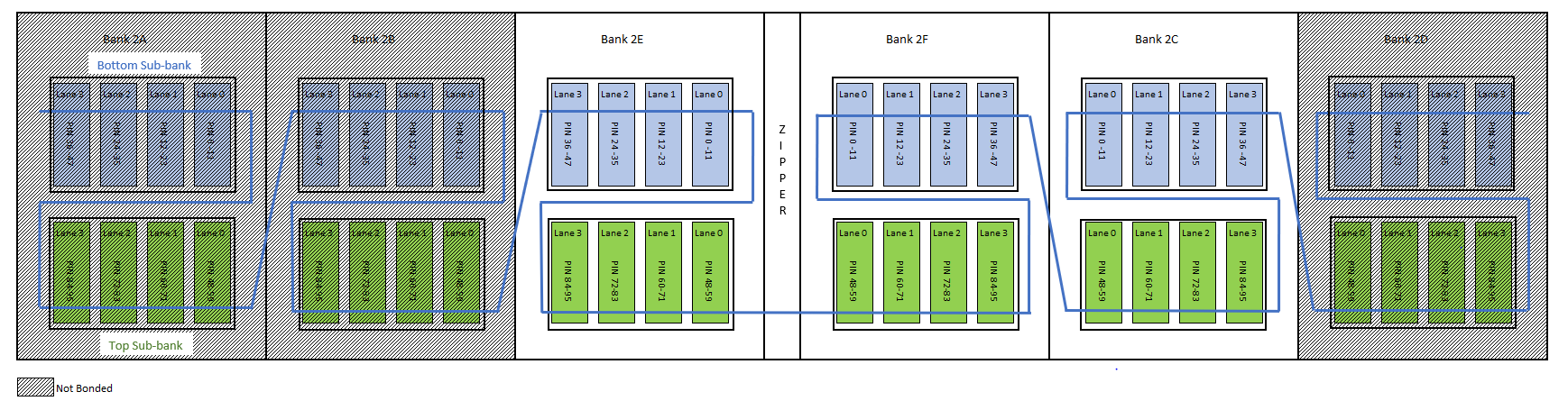
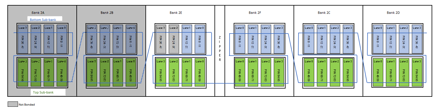
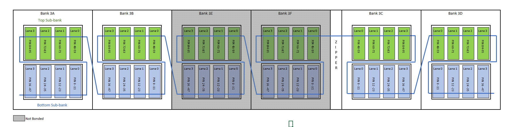
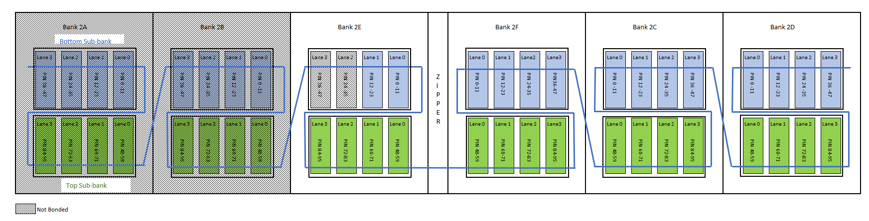
There are interconnects between the sub-banks which chain the sub-banks into a row. The following figures show how I/O lanes in various sub-banks are chained together to form the top and bottom I/O rows in various Intel® Agilex™ device variants. These figures represent the top view of the silicon die that corresponds to a reverse view of the device package.
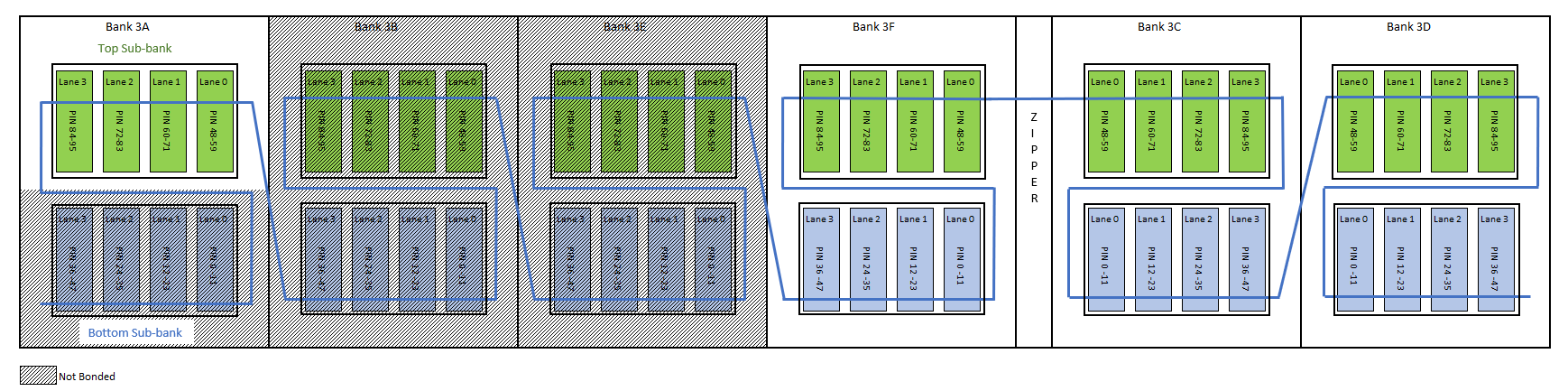
On the top I/O row in AGF022 and AGF027 package R25A , an EMIF interface cannot span across Bank 3A and Bank 3F, because the two I/O banks are not adjacent to each other.
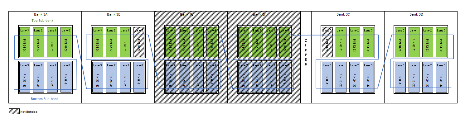
Bank 3E, Bank 3F, I/O Lane 0 in Top Sub-bank 3B and I/O Lane 0 in Top Sub-bank 3C are not bonded.
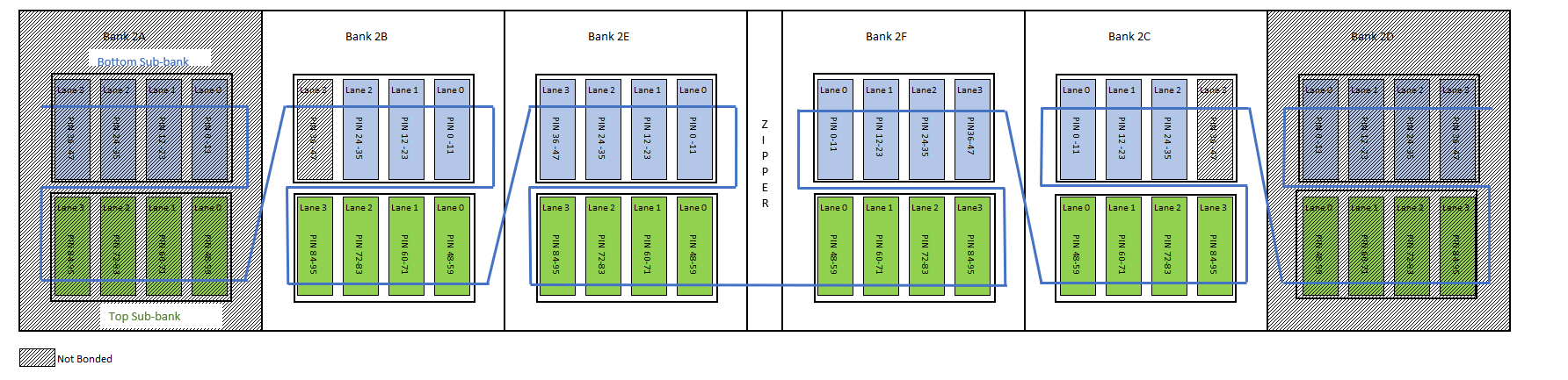
Bank 2A, Bank 2D, I/O Lane 3 in Bottom Sub-bank 2B and I/O Lane 3 in Bottom Sub-bank 2C are not bonded.
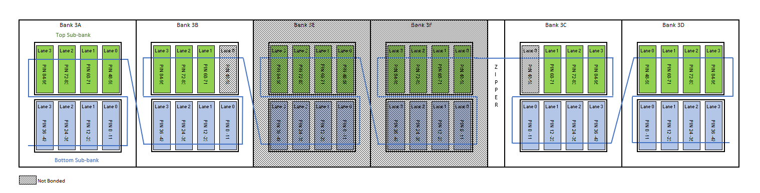
Bank 3E, Bank 3F, I/O Lane 0 in Top Sub-bank 3B and I/O Lane 0 in Top Sub-bank 3C are not bonded.
Bank 2A, Bank 2B, I/O Lane 3 and I/O Lane 2 in Bottom Sub-bank 2E are not bonded.

Bank 3E, Bank 3F, I/O Lane 0 in Top Sub-bank 3B and I/O Lane 0 in Top Sub-bank 3C are not bonded.

Bank 2A, Bank 2B, I/O Lane 3 and I/O Lane 2 in Bottom Sub-bank 2E are not bonded
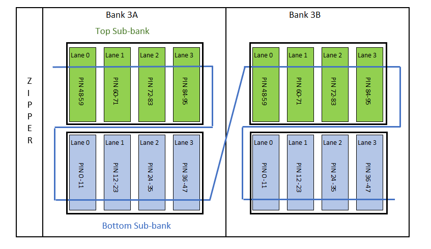
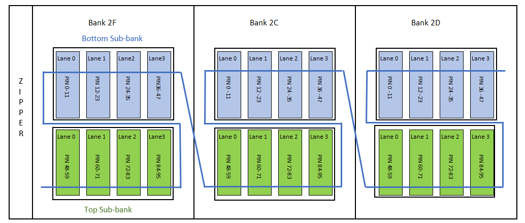
The two sub-banks within an I/O bank are adjacent to each other when there is at least one I/O lane in each sub-bank that is bonded out and available for EMIF use. The blue line in the above figures shows the connectivity between the sub-banks.
For example, in the top row in Intel® Agilex™ AGF012 and AGF014 devices (Figure 6):
- The top sub-bank in 3A is adjacent to the bottom sub-bank in 3A and the bottom sub-bank in 3B.
- The top sub-bank in 3B is adjacent to the bottom sub-bank in 3B and the top sub-bank in 3C.
- The top sub-bank in 3B is adjacent to the top sub-bank in 3C even though there is a zipper block between the two sub-banks.
- The top sub-bank in 3B is not adjacent to the bottom sub-bank in 3A.
When an interface must occupy multiple banks, ensure that those banks are adjacent to one another. You can identify where a pin is located within an I/O bank based on its Index within I/O Bank value in the device pinout file.
Zipper Block
The zipper is a block that performs necessary routing adjustments where routing wires cross the zipper.
I/O Sub-Bank Usage
The pins in an I/O bank can serve as address and command pins, data pins, or clock and strobe pins for an external memory interface. You can implement a narrow interface, DDR4 x8 interface, with only a single I/O sub-bank. A wider interface of up to 72 bits can be implemented by configuring multiple adjacent banks in a multi-bank interface.
Every sub-bank includes a hard memory controller which you can configure for DDR4. In a multi-bank interface, only the controller of one sub-bank is active; controllers in the remaining sub-banks are turned off to conserve power.
To use a multi-bank Intel® Agilex™ EMIF interface, you must observe the following rules:
- Designate one sub-bank as the address and command bank.
- The address and command sub-bank must contain all the address and command pins.
- The locations of individual address and command pins within the address and command sub-bank must adhere to the pin map defined in the pin table— regardless of whether you use the hard memory controller or not. You can find the pin tables at the following location: https://www.intel.com/content/www/us/en/programmable/support/literature/lit-dp.html.
- If you do use the hard memory controller, the address and command sub-bank contains the active hard controller.
All the sub-banks are capable of functioning as the address and command bank. For interfaces that span multiple sub-banks, the Intel® Quartus® Prime software requires that the address and command bank be placed in the center-most bank of the interface. The only exception to this rule is for the Hardened Processor Subsystem External Memory Interface.