Triple-Speed Ethernet IP Design Example User Guide: Agilex™ 3 and Agilex™ 5 FPGAs and SoCs
ID
813899
Date
8/04/2025
Public
A newer version of this document is available. Customers should click here to go to the newest version.
1. 10/100/1000 Ethernet MAC Design Example with 1000BASE-X/SGMII 2XTBI PCS with GTS Transceiver
2. 10/100/1000 Multiport Ethernet MAC Design Example with 1000BASE-X/SGMII PCS and Embedded PMA (LVDS)
3. 10/100/1000 Ethernet MAC without Internal FIFO Buffers with 1000BASE-X/SGMII 2XTBI PCS and Embedded PMA Signals (GTS) with IEEE 1588v2
4. 10/100/1000 Ethernet MAC without Internal FIFO Buffers with 1000BASE-X/SGMII TBI PCS and Embedded PMA Signals (LVDS I/O) with IEEE 1588v2
5. Triple-Speed Ethernet IP Design Example User Guide: Agilex™ 3 and Agilex™ 5 FPGAs and SoCs Archives
6. Document Revision History for the Triple-Speed Ethernet IP Design Example User Guide: Agilex™ 3 and Agilex™ 5 FPGAs and SoCs
3.2.5.1. Test Procedure
To turn on the System Console and test the hardware design example, follow these steps:
Note: You must connect the external loopback module to the QSFP28 port on bank 1A before running the test.
- In the Quartus® Prime Pro Edition software, select Tools > Programmer to configure the FPGA on the development board using the generated .sof file.
- In the Quartus® Prime Pro Edition software, select Tools > In-System Sources and Probes Editor.
- Set the phy_reset to 1 and reset_n to 0 to apply the reset.
- Set the phy_reset to 0 and reset_n to 1 to release the system from the reset state, as shown in the figure below.
Figure 25. In-System Sources and Probes Editor Setting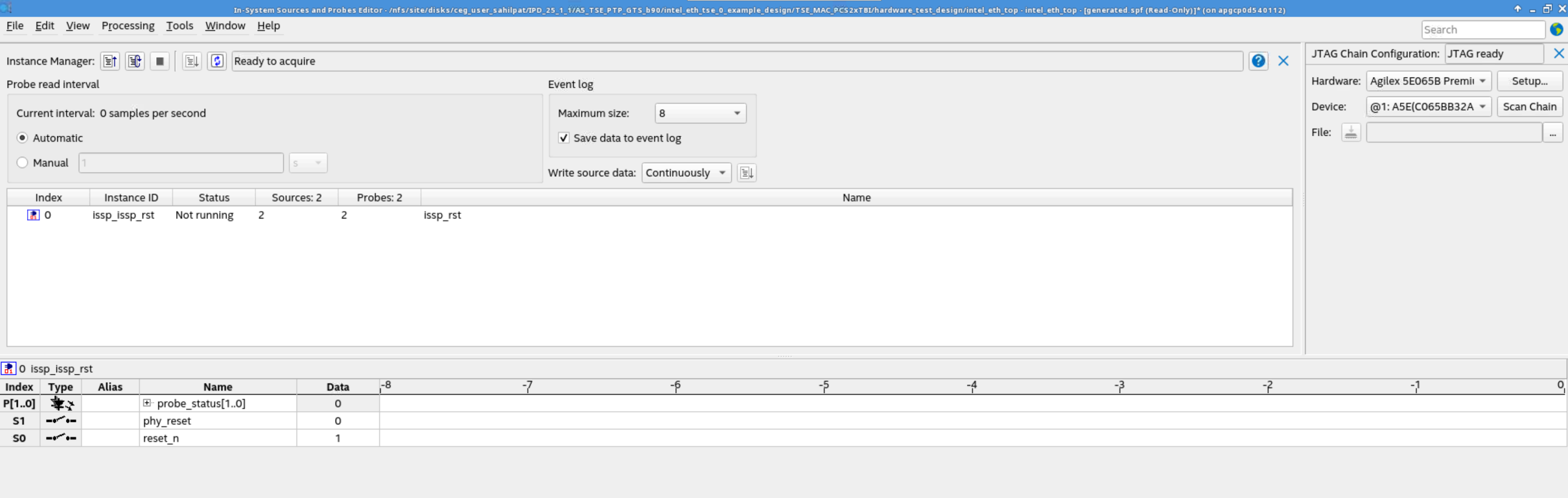
- In the Quartus® Prime Pro Edition software, select Tools > System Debugging Tools>System Console to launch the system console.
- In the Tcl Console pane, type cd hardware_test_design/sc to change directory to <design_example_dir>/TSE_MAC_PCS2xTBI/hardware_test_design/sc.
- Initialize the design command list by running this command: source main.tcl. If JTAG Master needs to be manually selected:
- Type list_jtag to display a list of JTAG master indexes that are connected to your board.
- Type set_jtag<number_of appropriate_JTAG_master> to select the JTAG master.
- Run the following loopback test:
TEST_SMA_LB <channel> <speed> <burst_size>
Example: TEST_SMA_LB 0 1G 1000
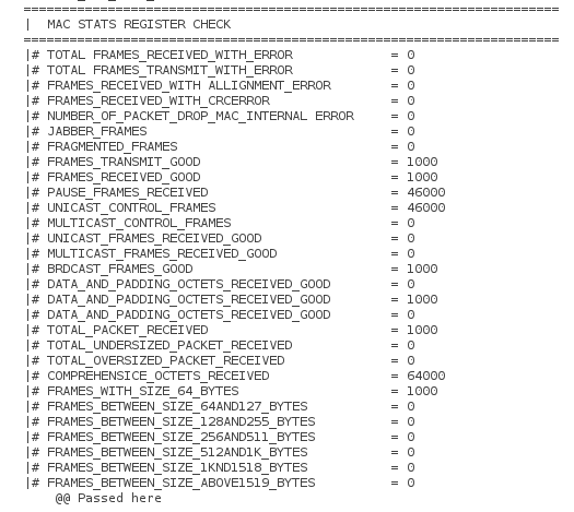
A successful test run displays the following message: