1. About the Nios® V Embedded Processor
2. Nios® V Processor Hardware System Design with Quartus® Prime Software and Platform Designer
3. Nios® V Processor Software System Design
4. Nios® V Processor Debugging, Verifying, and Simulating
5. Nios® V Processor Configuration and Booting Solutions
6. Finding Nios® V Processor Design Example
7. Nios® V Processor - Using the MicroC/TCP-IP Stack
8. Nios® V Processor — Remote System Update
9. Nios® V Processor — Using Custom Instruction
10. Nios® V Processor – Running TinyML Application
11. Nios® V Processor – Implementing Lockstep Capabilities
12. Nios® V Embedded Processor Design Handbook Archives
13. Document Revision History for the Nios® V Embedded Processor Design Handbook
2.1. Creating Nios® V Processor System Design with Platform Designer
2.2. Clocks and Resets Best Practices
2.3. Designing a Nios® V Processor Memory System
2.4. Assigning a UART Agent for Printing
2.5. Assigning a Default Agent
2.6. Understanding the Design Requirement with JTAG Signals
2.7. Optimizing Platform Designer System Performance
2.8. Integrating Platform Designer System into the Quartus® Prime Project
2.9. Handing Off to an Embedded FPGA Software Developer
4.2.3.2.1. Enabling Signal Tap Logic Analyzer
4.2.3.2.2. Adding Signals for Monitoring and Debugging
4.2.3.2.3. Specifying Trigger Conditions
4.2.3.2.4. Assigning the Acquisition Clock, Sample Depth, and Memory Type, and Buffer Acquisition Mode
4.2.3.2.5. Compiling the Design and Programming the Target Device
4.6.1. Prerequisites
4.6.2. Setting Up and Generating Your Simulation Environment in Platform Designer
4.6.3. Creating Nios V Processor Software
4.6.4. Generating Memory Initialization File
4.6.5. Generating System Simulation Files
4.6.6. Running Simulation in the QuestaSim Simulator Using Command Line
5.1. Introduction
5.2. Linking Applications
5.3. Nios® V Processor Booting Methods
5.4. Introduction to Nios® V Processor Booting Methods
5.5. Nios® V Processor Booting from On-Chip Flash (UFM)
5.6. Nios® V Processor Booting from General Purpose QSPI Flash
5.7. Nios® V Processor Booting from Configuration QSPI Flash
5.8. Nios® V Processor Booting from On-Chip Memory (OCRAM)
5.9. Nios® V Processor Booting from Tightly Coupled Memory (TCM)
5.10. Summary of Nios® V Processor Vector Configuration and BSP Settings
5.11. Reducing Nios® V Processor Booting Time
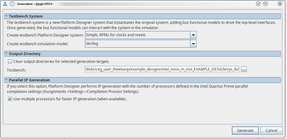
4.6.2. Setting Up and Generating Your Simulation Environment in Platform Designer
To generate simulation files, perform the following steps:
- Start the Intel Quartus Prime software and open the Platform Designer from the Tools menu.
- Open the <your project design>.qsys file.
Note: Ensure that you have completed building your Platform Designer system before generating the simulation models
- In Platform Designer, navigate to Generate > Generate Testbench System.
- On the Generation window, set the following parameters to these values:
- Create testbench Platform Designer system— Standard, BFMs for standard Platform Designer interfaces.
Note: If your system has exported ports other than the clock and reset, choose Standard, BFMs for standard Avalon interfaces.
- Create testbench simulation model—Verilog
- Select Use multiple processors for faster IP generation (when available).
- Create testbench Platform Designer system— Standard, BFMs for standard Platform Designer interfaces.
- Click Generate, and Save, if prompted.
Figure 40. Testbench Generation