1. About the Nios® V Embedded Processor
2. Nios® V Processor Hardware System Design with Quartus® Prime Software and Platform Designer
3. Nios® V Processor Software System Design
4. Nios® V Processor Debugging, Verifying, and Simulating
5. Nios® V Processor Configuration and Booting Solutions
6. Finding Nios® V Processor Design Example
7. Nios® V Processor - Using the MicroC/TCP-IP Stack
8. Nios® V Processor — Remote System Update
9. Nios® V Processor — Using Custom Instruction
10. Nios® V Processor – Running TinyML Application
11. Nios® V Processor – Implementing Lockstep Capabilities
12. Nios® V Embedded Processor Design Handbook Archives
13. Document Revision History for the Nios® V Embedded Processor Design Handbook
2.1. Creating Nios® V Processor System Design with Platform Designer
2.2. Clocks and Resets Best Practices
2.3. Designing a Nios® V Processor Memory System
2.4. Assigning a UART Agent for Printing
2.5. Assigning a Default Agent
2.6. Understanding the Design Requirement with JTAG Signals
2.7. Optimizing Platform Designer System Performance
2.8. Integrating Platform Designer System into the Quartus® Prime Project
2.9. Handing Off to an Embedded FPGA Software Developer
4.2.3.2.1. Enabling Signal Tap Logic Analyzer
4.2.3.2.2. Adding Signals for Monitoring and Debugging
4.2.3.2.3. Specifying Trigger Conditions
4.2.3.2.4. Assigning the Acquisition Clock, Sample Depth, and Memory Type, and Buffer Acquisition Mode
4.2.3.2.5. Compiling the Design and Programming the Target Device
4.6.1. Prerequisites
4.6.2. Setting Up and Generating Your Simulation Environment in Platform Designer
4.6.3. Creating Nios V Processor Software
4.6.4. Generating Memory Initialization File
4.6.5. Generating System Simulation Files
4.6.6. Running Simulation in the QuestaSim Simulator Using Command Line
5.1. Introduction
5.2. Linking Applications
5.3. Nios® V Processor Booting Methods
5.4. Introduction to Nios® V Processor Booting Methods
5.5. Nios® V Processor Booting from On-Chip Flash (UFM)
5.6. Nios® V Processor Booting from General Purpose QSPI Flash
5.7. Nios® V Processor Booting from Configuration QSPI Flash
5.8. Nios® V Processor Booting from On-Chip Memory (OCRAM)
5.9. Nios® V Processor Booting from Tightly Coupled Memory (TCM)
5.10. Summary of Nios® V Processor Vector Configuration and BSP Settings
5.11. Reducing Nios® V Processor Booting Time
5.8.1.1. Hardware Design Flow
The following sections describe a step-by-step method for building a bootable system for a Nios® V processor application from OCRAM. The example below is built using Intel Arria 10 SoC development kit.
IP Component Settings
- Create your Nios® V processor project using Quartus® Prime and Platform Designer.
- Ensure the On-Chip Memory (RAM or ROM) Altera FPGA is added into your Platform Designer system.
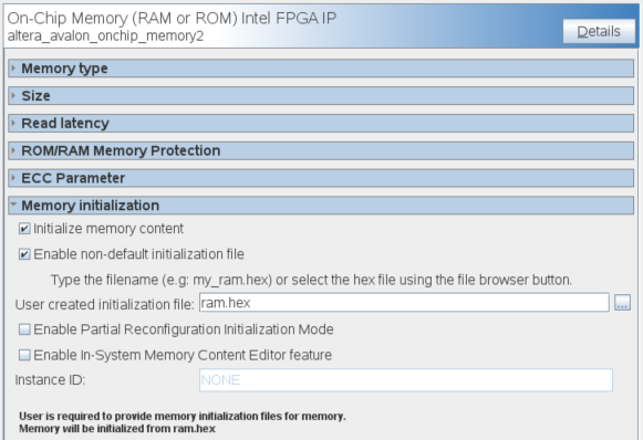
- Enable Initialize memory content and Enable non-default initialization file with ram.hex in the on-chip memory.
Figure 167. Connections for Nios® V Processor Project
Figure 168. On-Chip Memory (RAM or ROM) Intel FPGA IP Parameter Settings
Reset Agent Settings for Nios® V Processor
- In the Nios® V processor parameter editor, set the Reset Agent to OCRAM
Figure 169. Nios® V Processor Parameter Editor Settings
- Click Generate HDL, the Generation dialog box appears.
- Specify output file generation options and then click Generate.
Quartus® Prime Settings
- In the Intel Quartus Prime software, click Assignment > Device > Device and Pin Options > Configuration.
- Set Configuration scheme according to your FPGA configuration scheme
- Click OK to exit the Device and Pin Options window.
- Click OK to exit the Device window.
- Click Start Compilation to compile your project.
Related Information