F-Tile Architecture and PMA and FEC Direct PHY IP User Guide
ID
683872
Date
1/24/2025
Public
A newer version of this document is available. Customers should click here to go to the newest version.
1. F-Tile Overview
2. F-Tile Architecture
3. Implementing the F-Tile PMA/FEC Direct PHY Intel® FPGA IP
4. Implementing the F-Tile Reference and System PLL Clocks Intel® FPGA IP
5. F-Tile PMA/FEC Direct PHY Design Implementation
6. Supported Tools
7. Debugging F-Tile Transceiver Links
8. F-Tile Architecture and PMA and FEC Direct PHY IP User Guide Archives
9. Document Revision History for the F-Tile Architecture and PMA and FEC Direct PHY IP User Guide
A. Appendix
2.1.1. FHT and FGT PMAs
2.1.2. 400G Hard IP and 200G Hard IP
2.1.3. PMA Data Rates
2.1.4. FEC Architecture
2.1.5. PCIe* Hard IP
2.1.6. Bonding Architecture
2.1.7. Deskew Logic
2.1.8. Embedded Multi-die Interconnect Bridge (EMIB)
2.1.9. IEEE 1588 Precision Time Protocol for Ethernet
2.1.10. Clock Networks
2.1.11. Reconfiguration Interfaces
2.2.1. PMA-to-Fracture Mapping
2.2.2. Determining Which PMA to Map to Which Fracture
2.2.3. Hard IP Placement Rules
2.2.4. IEEE 1588 Precision Time Protocol Placement Rules
2.2.5. Topologies
2.2.6. FEC Placement Rules
2.2.7. Clock Rules and Restrictions
2.2.8. Bonding Placement Rules
2.2.9. Preserving Unused PMA Lanes
2.2.2.1. Implementing One 200GbE-4 Interface with 400G Hard IP and FHT
2.2.2.2. Implementing One 200GbE-2 Interface with 400G Hard IP and FHT
2.2.2.3. Implementing One 100GbE-1 Interface with 400G Hard IP and FHT
2.2.2.4. Implementing One 100GbE-4 Interface with 400G Hard IP and FGT
2.2.2.5. Implementing One 10GbE-1 Interface with 200G Hard IP and FGT
2.2.2.6. Implementing Three 25GbE-1 Interfaces with 400G Hard IP and FHT
2.2.2.7. Implementing One 50GbE-1 and Two 25GbE-1 Interfaces with 400G Hard IP and FHT
2.2.2.8. Implementing One 100GbE-1 and Two 25GbE-1 Interfaces with 400G Hard IP and FHT
2.2.2.9. Implementing Two 100GbE-1 and One 25GbE-1 Interfaces with 400G Hard IP and FHT
2.2.2.10. Implementing 100GbE-1, 100GbE-2, and 50GbE-1 Interfaces with 400G Hard IP and FHT
3.1. F-Tile PMA/FEC Direct PHY Intel® FPGA IP Overview
3.2. Designing with F-Tile PMA/FEC Direct PHY Intel® FPGA IP
3.3. Configuring the IP
3.4. Signal and Port Reference
3.5. Bit Mapping for PMA and FEC Mode PHY TX and RX Datapath
3.6. Clocking
3.7. Custom Cadence Generation Ports and Logic
3.8. Asserting Reset
3.9. Bonding Implementation
3.10. Independent Port Configurations
3.11. Configuration Registers
3.12. Configurable Quartus® Prime Software Settings
3.13. Configuring the F-Tile PMA/FEC Direct PHY Intel® FPGA IP for Hardware Testing
3.14. Hardware Configuration Using the Avalon® Memory-Mapped Interface
3.3.1. General and Common Datapath Options
3.3.2. TX Datapath Options
3.3.3. RX Datapath Options
3.3.4. RS-FEC (Reed Solomon Forward Error Correction) Options
3.3.5. Avalon® Memory Mapped Interface Options
3.3.6. Register Map IP-XACT Support
3.3.7. Example Design Generation
3.3.8. Analog Parameter Options
3.4.1. TX and RX Parallel and Serial Interface Signals
3.4.2. TX and RX Reference Clock and Clock Output Interface Signals
3.4.3. Reset Signals
3.4.4. RS-FEC Signals
3.4.5. Custom Cadence Control and Status Signals
3.4.6. TX PMA Control Signals
3.4.7. RX PMA Status Signals
3.4.8. TX and RX PMA and Core Interface FIFO Signals
3.4.9. PMA Avalon® Memory Mapped Interface Signals
3.4.10. Datapath Avalon® Memory Mapped Interface Signals
3.5.1. Parallel Data Mapping Information
3.5.2. TX and RX Parallel Data Mapping Information for Different Configurations
3.5.3. Example of TX Parallel Data for PMA Width = 8, 10, 16, 20, 32 (X=1)
3.5.4. Example of TX Parallel Data for PMA width = 64 (X=2)
3.5.5. Example of TX Parallel Data for PMA width = 64 (X=2) for FEC Direct Mode
3.8.1. Reset Signal Requirements
3.8.2. Power On Reset Requirements
3.8.3. Reset Signals—Block Level
3.8.4. Reset Signals—Descriptions
3.8.5. Status Signals—Descriptions
3.8.6. Run-time Reset Sequence—TX
3.8.7. Run-time Reset Sequence—RX
3.8.8. Run-time Reset Sequence—TX + RX
3.8.9. Run-time Reset Sequence—TX with FEC
4.1. IP Parameters
4.2. IP Port List
4.3. Mode of System PLL - System PLL Reference Clock and Output Frequencies
4.4. Guidelines for F-Tile Reference and System PLL Clocks Intel® FPGA IP Usage
4.5. Guidelines for Refclk #i is Active At and After Device Configuration
4.6. Guidelines for Obtaining the Lock Status and Resetting the FGT and FHT TX PLLs
5.1. Implementing the F-Tile PMA/FEC Direct PHY Design
5.2. Instantiating the F-Tile PMA/FEC Direct PHY Intel® FPGA IP
5.3. Implementing a RS-FEC Direct Design in the F-Tile PMA/FEC Direct PHY Intel® FPGA IP
5.4. Instantiating the F-Tile Reference and System PLL Clocks Intel® FPGA IP
5.5. Enabling Custom Cadence Generation Ports and Logic
5.6. Connecting the F-Tile PMA/FEC Direct PHY Design IP
5.7. Simulating the F-Tile PMA/FEC Direct PHY Design
5.8. F-Tile Interface Planning
7.2.1. Modifying the Design to Enable F-Tile Transceiver Debug
7.2.2. Programming the Design into an Intel FPGA
7.2.3. Loading the Design to the Transceiver Toolkit
7.2.4. Creating Transceiver Links
7.2.5. Running BER Tests
7.2.6. Running Eye Viewer Tests
7.2.7. Running Link Optimization Tests
7.2.8. Checking FEC Statistics
7.2.9. Vertical Bathtub Curve Measurements (VBCM) Data
5.4. Instantiating the F-Tile Reference and System PLL Clocks Intel® FPGA IP
The F-Tile Reference and System PLL Clocks Intel® FPGA IP is required for F-tile PMA/FEC Direct PHY designs. You must instantiate and connect this IP for simulation and compilation.
This design requires the following for the F-Tile Reference and System PLL Clocks Intel® FPGA IP:
- System PLL mode and reference clock source for one system PLL that clocks the datapath.
- Reference clock source for FGT PMA. Share or separate the reference clock source for system PLL and FGT PMA. This example shares the reference clock.
To specify the system PLL mode and reference clock source for one system PLL:
- In the IP Catalog search field, type f-tile Reference, and double-click the F-Tile Reference and System PLL Clocks Intel® FPGA IP under Transceiver PHY.
- On the System PLL #0 tab, specify the following:
Table 113. System PLL #0 Options Parameter Parameter Value Mode of system PLL Select ETHERNET_FREQ_830_156. This configures the system PLL input frequency to 156.25 MHz and output frequency to 830.078125 MHz (must match system PLL frequency in F-Tile PMA/FEC Direct PHY Intel® FPGA IP). Refclk source RefClk #0. Selects the reference clock source for system PLL. RefClk #0 for FGT PMA On - Under RefClk, specify the following options:
Table 114. RefClk Options Parameter Parameter Value Enable RefClk #0 for FGT PMA On. This reference clock is shared between system PLL #0 and FGT PMA RefClk source RefClk #0. 156.25 MHz (same as reference clock frequency for F-Tile PMA/FEC Direct PHY Intel® FPGA IP).
Figure 108. System PLL and RefClk Options
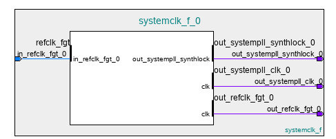
The following figures shows the block symbol and available ports for F-Tile Reference and System PLL Clocks Intel® FPGA IP in this example
Figure 109. Example F-Tile Reference and System PLL Clocks Intel® FPGA IP Ports