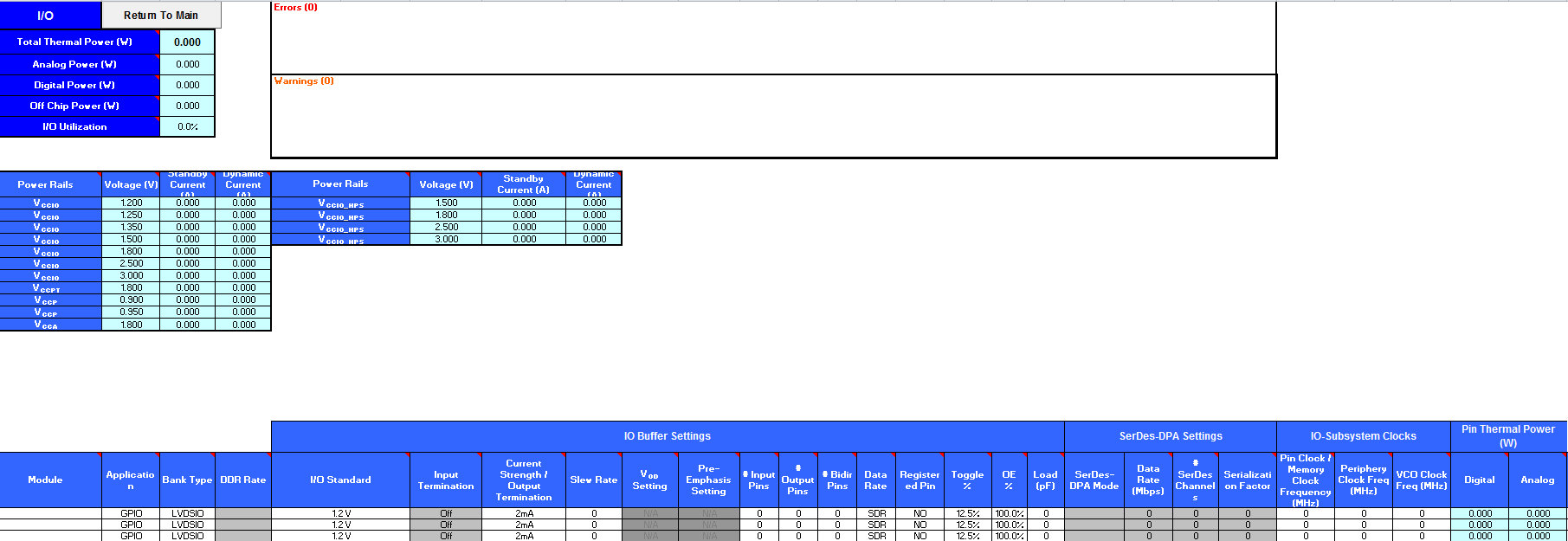
4.8. Arria® 10 EPE - I/O Worksheet
When using the EPE spreadsheet, it is assumed you are using external termination resistors as recommended for SSTL and high-speed transceiver logic HSTL. If your design does not use external termination resistors, choose the LVTTL/ LVCMOS I/O standard with the same VCCIO and similar current strength as the terminated I/O standard. For example, if you are using the SSTL-2 Class II I/O standard with a 16 mA current strength, you must select 2.5 V as the I/O standard and 16 mA as the current strength in the EPE spreadsheet.
To use on-chip termination (OCT), select the Current Strength/Output Termination option in the EPE spreadsheet.
The power reported for the I/O signals includes thermal and external I/O power. The total thermal power is the sum of the thermal power consumed by the device from each power rail, as shown in the following equation.
The following figure shows the I/O power consumption. The ICCIO power rail includes both the thermal PIO and the external PIO.
The VREF pins consume minimal current (typically less than 10 μA) and is negligible when compared with the current consumed by the general purpose I/O (GPIO) pins; therefore, the EPE spreadsheet does not include the current for VREF pins in the calculations.
| Column Heading | Description |
|---|---|
| Module | Specify a name for the I/O in this column. This is an optional value. |
| Application | Specify the application for this I/O row. GPIO and SerDes interfaces can be instantiated using this field. Use the IP worksheet to instantiate EMIF interfaces. |
| Bank Type | Specifies the type of I/O bank for this row. An LVDSIO bank supports I/O standards up to 1.8V as well as LVDS I/O standards. 3V I/O banks support I/O standards up to 3.0V but not LVDS I/O standards. |
| DDR Rate | Specifies the clock rate of PHY logic. Determines the clock frequency of PHY logic in relation to the memory clock frequency. For example, if the memory clock sent from the FPGA to the memory device is toggling at 800MHz, a quarter rate interface means that the PHY logic in the FPGA runs at 200MHz. |
| I/O Buffer Settings - I/O Standard | Specifies the I/O standard used by the I/O pins in this module. |
| I/O Buffer Settings - Input Termination | Specifies the input termination setting for the input and bidirectional pins in this module. |
| I/O Buffer Settings - Current Strength/Output Termination | Specifies the current strength or output termination setting for the output and bidirectional pins in this module. Current strength and output termination are mutually exclusive. |
| I/O Buffer Settings - Slew Rate | Specifies the slew rate setting for the output and bidirectional pins in this module. Using a lower slew rate setting helps reduce switching noise but may increase delay. |
| I/O Buffer Settings - VOD Setting | Specifies the differential output voltage (VOD) for the output and bidirectional pins in the module. A smaller number indicates a smaller VOD which reduces static power. |
| I/O Buffer Settings - Pre-Emphasis Setting | Specifies the pre-emphasis setting for the output and bidirectional pins in this module. A smaller number indicates a smaller pre-emphasis which reduces dynamic power. |
| I/O Buffer Settings - # Input Pins | Specifies the number of input-only I/O pins in this module. Differential pin pairs count as one pin. |
| I/O Buffer Settings - # Output Pins | Specifies the number of output-only I/O pins in this module. Differential pin pairs count as one pin. |
| I/O Buffer Settings - # Bidir Pins | Specifies the number of bidirectional I/O pins in this module. Differential pin pairs count as one pin. The I/O pin is treated as an output when its output enable signal is active and is treated as an input when the output enable signal is disabled. An I/O pin configured as a bidirectional pin, but used only as an output, consumes more power than if it were configured as an output-only pin, due to the toggling of the input buffer every time the output buffer toggles (they share a common pin). |
| I/O Buffer Settings - Data Rate | Indicates whether I/O value will change once (Single-Data Rate) or twice (Double-Data Rate) per cycle. |
| I/O Buffer Settings - Registered Pin | Indicates whether the pin is registered or not. |
| I/O Buffer Settings - Toggle % | Percentage of clock cycles when the I/O signal changes value. This value is multiplied by clock frequency to determine the number of transitions per second. If DDR is selected, the toggle rate is multiplied by an additional factor of two. |
| I/O Buffer Settings - OE % | For modules with Input Termination set to OFF, enter the average percentage of time that:
During the remaining time:
Input Termination cannot be active while the Output I/O is enabled, so for modules with Input Termination not set to OFF, enter the average percentage of time that On-Chip Termination is inactive (that is, 1-percentage that the On-Chip Termination is active).This number must be a percentage between 0% and 100%. |
| I/O Buffer Settings - Load (pF) | Specifies pin loading external to the chip (in pF). Applies only to outputs and bidirectional pins. Pin and package capacitance is already included in the I/O model. Include only off-chip capacitance. |
| SerDes-DPA Settings - SerDes-DPA Mode | Selects the mode of SerDes-DPA block. |
| SerDes-DPA Settings - Data Rate (Mbps) | The maximum data rate of the SerDes channels in Mbps. |
| SerDes-DPA Settings - # SerDes Channels | The number of channels running at the data rate of this SerDes domain. |
| SerDes-DPA Settings - Serialization Factor | Number of parallel data bits for each serial data bit. |
| I/O Subsystem Clocks - Pin Clock/Memory Clock Frequency (MHz) | Clock frequency (in MHz). 100 MHz with a 12.5% toggle percentage would mean that each I/O pin toggles 12.5 million times per second (100 MHz * 12.5%). |
| I/O Subsystem Clocks - Periphery Clock Freq (MHz) | The I/O subsystem internal PHY clock frequency. This is an output-only field. In SerDes applications, the PHY clock frequency is a function of the SerDes rate and serialization factor. In external memory interface (EMIF) applications, the PHY clock frequency is a function of the memory clock frequency and DDR rate of the EMIF IP. |
| I/O Subsystem Clocks - VCO Clock Freq (MHz) | The internal VCO operating frequency. This is an output-only field. In SerDes applications, VCO frequency is a function of SerDes Data rate. In external memory interface (EMIF) applications, the VCO frequency is a function of the memory clock frequency of the EMIF IP. The VCO frequency is not applicable in GPIO mode. |
| Pin Thermal Power (W) - Digital | Power dissipated in the digital domain of the I/O-subsystem including GPIO, EMIF controller and SerDes controller. |
| Pin Thermal Power (W) - Analog | Power dissipated in the analog domain of the I/O-subsystem, for example, I/O buffers. |
| User Comments | Enter any comments. This is an optional entry. |
For more information about the I/O standard termination schemes, refer to I/O and High Speed I/Os in Arria® 10 Devices.