L-Tile and H-Tile Avalon® Memory-mapped Intel® FPGA IP for PCI Express* User Guide
ID
683667
Date
9/13/2024
Public
1. Introduction
2. Quick Start Guide
3. Interface Overview
4. Parameters
5. Designing with the IP Core
6. Block Descriptions
7. Registers
8. Programming Model for the DMA Descriptor Controller
9. Programming Model for the Avalon® -MM Root Port
10. Avalon-MM Testbench and Design Example
11. Document Revision History
A. PCI Express Core Architecture
B. Root Port Enumeration
C. Troubleshooting and Observing the Link Status
2.1. Design Components
2.2. Hardware and Software Requirements
2.3. Directory Structure
2.4. Generating the Design Example
2.5. Simulating the Design Example
2.6. Compiling the Design Example and Programming the Device
2.7. Installing the Linux Kernel Driver
2.8. Running the Design Example Application
7.1.1. Register Access Definitions
7.1.2. PCI Configuration Header Registers
7.1.3. PCI Express Capability Structures
7.1.4. Intel Defined VSEC Capability Header
7.1.5. Uncorrectable Internal Error Status Register
7.1.6. Uncorrectable Internal Error Mask Register
7.1.7. Correctable Internal Error Status Register
7.1.8. Correctable Internal Error Mask Register
7.2.1.1. Avalon-MM to PCI Express Interrupt Status Registers
7.2.1.2. Avalon-MM to PCI Express Interrupt Enable Registers
7.2.1.3. Address Mapping for High-Performance Avalon-MM 32-Bit Slave Modules
7.2.1.4. PCI Express to Avalon-MM Interrupt Status and Enable Registers for Endpoints
7.2.1.5. PCI Express Configuration Information Registers
10.5.1. ebfm_barwr Procedure
10.5.2. ebfm_barwr_imm Procedure
10.5.3. ebfm_barrd_wait Procedure
10.5.4. ebfm_barrd_nowt Procedure
10.5.5. ebfm_cfgwr_imm_wait Procedure
10.5.6. ebfm_cfgwr_imm_nowt Procedure
10.5.7. ebfm_cfgrd_wait Procedure
10.5.8. ebfm_cfgrd_nowt Procedure
10.5.9. BFM Configuration Procedures
10.5.10. BFM Shared Memory Access Procedures
10.5.11. BFM Log and Message Procedures
10.5.12. Verilog HDL Formatting Functions
8.1. Read DMA Example
This example moves three data blocks from the PCIe address space (system memory) to the Avalon-MM address space.
Note: Beginning with the 17.1 release, the Quartus® Prime Pro Edition software dynamically generates example designs for the parameters you specify in the using the parameter editor. Consequently, the Quartus® Prime Pro Edition installation directory no longer provides static example designs for Stratix® 10 devices. Static example designs are available for earlier device families, including Arria® 10 and Cyclone® 10 devices.
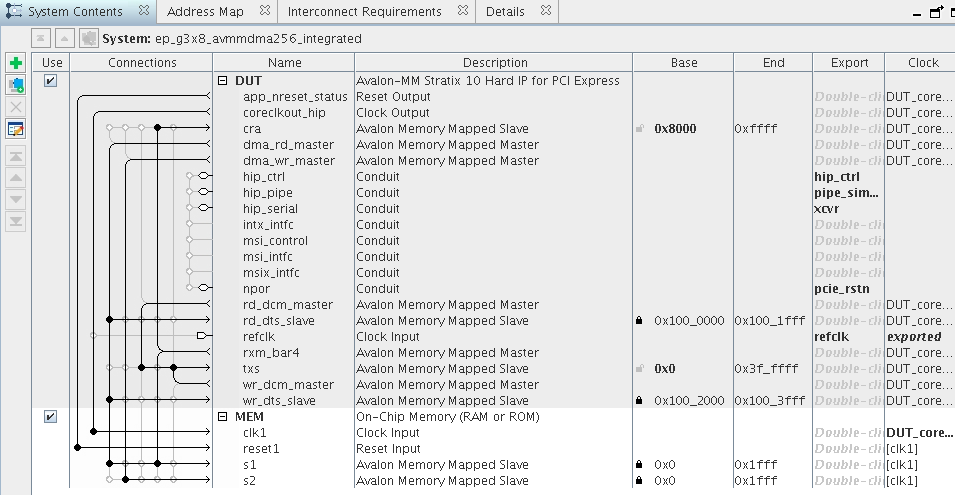
Figure 59. Stratix® 10 Gen3 x8 Avalon-MM DMA Integrated Platform Designer
The following figures illustrate the location and size of the data blocks in the PCIe and Avalon® -MM address spaces and the descriptor table format. In this example, the value of RD_TABLE_SIZE is 127.
Figure 60. Data Blocks to Transfer from PCIe to Avalon-MM Address Space Using Read DMA
The descriptor table includes 128 entries. The status table precedes a variable number of descriptors in memory. The Read and Write Status and Descriptor Tables are at the address specified in the Read Descriptor Base Register and Write Descriptor Base Register, respectively.
Figure 61. Descriptor Table In PCIe* System Memory
- Software allocates memory for the Read Descriptor Status table and Descriptor table in PCIe* system memory. The memory allocation requires the following calculation:
- Each entry in the read status table is 4 bytes. The 128 read entries require 512 bytes of memory.
- Each descriptor is 32 bytes. The three descriptors require 96 bytes of memory.
Note: To avoid a possible overflow condition, allocate the memory needed for the number of descriptors supported by RD_TABLE_SIZE, rather than the initial number of descriptors.
The total memory that software must allocate for the status and descriptor tables is 608 bytes. The start address of the allocated memory in this example is 0xF000_0000. Write this address into the Read Descriptor Controller Read Status and Descriptor Base registers. - Program the Read Descriptor Controller table starting at offset 0x200 from the Read Status and Descriptor Base. This offset matches the addresses shown in Data Blocks to Transfer from PCIe to Avalon-MM Address Space Using Read DMA. The three blocks of data require three descriptors.
- Program the Read Descriptor Controller Read Status and Descriptor Base register with the starting address of the descriptor status table.
- Program the Read Descriptor Controller Read Descriptor FIFO Base with the starting address of the on-chip descriptor table FIFO. This is the base address for the rd_dts_slave port in Platform Designer. In this example, the address is 0x0100_0000.
Figure 62. Address of the On-Chip Read FIFO
- To get status updates for each descriptor, program the Read Descriptor Controller RD_CONTROL register with 0x1. This step is optional.
- Program the Read Descriptor Controller register RD_DMA_LAST_PTR with the value 3. Programming this register triggers the Read Descriptor Controller descriptor table fetch process. Consequently, writing this register must be the last step in setting up DMA transfers.
- The host waits for the MSI interrupt. The Read Descriptor Controller sends the MSI to the host after completing the last descriptor. The Read Descriptor Controller also writes the Update.
- If there are additional blocks of data to move, complete the following steps to set up additional transfers.
- Program the descriptor table starting from memory address 0xF000_0200 + (<previous last descriptor pointer> * 0x20). In this case the descriptor pointer was 3.
- Program the Read Descriptor Controller register RD_DMA_LAST_PTR with previous_value (3 in this case) + number of new descriptors. Programming this register triggers the Read Descriptor Controller descriptor table fetch process. Consequently, programming this register must be the last step in setting up DMA transfers.
Note: When RD_DMA_LAST_PTR approaches the RD_TABLE_SIZE, be sure to program the RD_DMA_LAST_PTR with a value equal to RD_TABLE_SIZE. Doing so ensures that the rollover to the first descriptor at the lowest offset occurs, (0xF000_0200 in this example). Refer to the description of the RD_DMA_LAST_PTR in the Read DMA Descriptor Controller Registers section for further information about programming the RD_DMA_LAST_PTR register.
Related Information