Multi Channel DMA Intel® FPGA IP for PCI Express Design Example User Guide
ID
683517
Date
10/28/2022
Public
A newer version of this document is available. Customers should click here to go to the newest version.
3.5.2.6.1. Build and Install Netdev Driver
3.5.2.6.2. Enable VFs if SRIOV is Supported
3.5.2.6.3. Configure the Number of Channels Supported on the Device
3.5.2.6.4. Configure the MTU Value
3.5.2.6.5. Configure the Device Communication
3.5.2.6.6. Configure Transmit Queue Selection Mechanism
3.5.2.6.7. Test Procedure by Using Name Space Environment
3.5.2.6.8. PIO Test
3.3.1. Testbench Overview
Figure 24. Testbench Platform Designer View
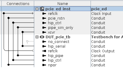
The design example, pcie_ed_inst, is generated with the link width you select in the IP Parameter Editor. The Intel FPGA BFM, DUT_pcie_tb, is a Root Port BFM.
Note: The H-Tile Root Port BFM only supports up to Gen3 x8 width and downtrains x16 Endpoint to Gen3 x8. If you want to simulate x16 link width with MCMDA H-Tile Endpoint, you can use a third-party Root Complex BFM.
The testbench uses a Root Port driver module to initiate the configuration and exercise the target memory and DMA channel in the Endpoint. This is the module that you can modify to vary the transactions sent to the example Endpoint design or your own design.
The driver module path and file is as follows:
- MCDMA P-Tile testbench
Path: pcie_ed_tb/ip/pcie_ed_tb/DUT_pcie_tb_ip/intel_pcie_ptile_tbed_100/sim
File: altpcietb_bfm_rp_gen4_x16.sv
- MCDMA F-Tile testbench
Path: pcie_ed_tb/ip/pcie_ed_tb/dut_pcie_tb_ip/intel_pcie_ftile_tbed_100/sim
File: altpcietb_bfm_rp_gen4_x16.sv
- MCDMA H-Tile testbench
Path: pcie_ed_tb/ip/pcie_ed_tb/DUT_pcie_tb_ip/altera_pcie_s10_tbed_191/sim
File: altpcietb_bfm_rp_gen3_x8.sv
For more information about Intel FPGA BFM, refer to the Testbench overview in the user guides provided below: