AN 890: JESD204B Intel® FPGA IP and ADI AD9174 Interoperability Report for Intel Stratix® 10 L-Tile Devices
1.5. Test Results
The following table contains the possible results and their definition.
| Result | Definition |
|---|---|
| PASS | The device under test (DUT) was observed to exhibit conformant behavior. |
| PASS with comments | The DUT was observed to exhibit conformant behavior. However, an additional explanation of the situation is included (example: due to time limitations, only a portion of the testing was performed). |
| FAIL | The DUT was observed to exhibit non-conformant behavior. |
| Warning | The DUT was observed to exhibit behavior that is not recommended. |
| Refer to comments | From the observations, a valid pass or fail could not be determined. An additional explanation of the situation is included. |
The following table shows the results for test cases CGS.1, CGS.2, ILA.1, ILA.2, ILA.3, TL.1, TL.2, SCR.1, and SCR.2 with K = 32, subclass 1, and different values of L, M, F, data rate, sampling clock, link clock, and SYSREF pulse frequency.
| Test No. | L | M | F | SCR9 | Lane Rate (Gbps) | DAC Rate (Msps) | Link Clock (MHz) | SYSREF Pulse Frequency (MHz) | Result |
|---|---|---|---|---|---|---|---|---|---|
| 1 | 1 | 2 | 4 | 0 | 14.7456 | 5898.24 | 368.64 | 11.52 | PASS |
| 2 | 1 | 2 | 4 | 1 | 14.7456 | 5898.24
|
368.64 | 11.52 | PASS |
| 3 | 2 | 4 | 4 | 0 | 14.7456 | 11796.48 | 368.64 | 11.52 | PASS |
| 4 | 2 | 4 | 4 | 1 | 14.7456 | 11796.48 | 368.64 | 11.52 | PASS |
| 5 | 3 | 6 | 4 | 0 | 14.7456 | 11796.48 | 368.64 | 11.52 | PASS |
| 6 | 3 | 6 | 4 | 1 | 14.7456 | 11796.48 | 368.64 | 11.52 | PASS |
| 7 | 2 | 2 | 2 | 0 | 14.7456 | 5898.24 | 368.64 | 23.04 | PASS |
| 8 | 2 | 2 | 2 | 1 | 14.7456 | 5898.24 | 368.64 | 23.04 | PASS |
| 9 |
4 | 4 | 2 | 0 | 14.7456 | 11796.48 | 368.64 | 23.04 | PASS |
| 10 | 4 | 4 | 2 | 1 | 14.7456 | 11796.48 | 368.64 | 23.04 | PASS |
| 11 | 1 | 2 | 3 | 0 | 14.7456 | 11796.48 | 368.64 | 15.36 | PASS |
| 12 | 1 | 2 | 3 | 1 | 14.7456 | 11796.48 | 368.64 | 15.36 | PASS |
| 13 | 2 | 4 | 3 | 0 | 14.7456 | 11796.48 | 368.64 | 15.36 | PASS |
| 14 | 2 | 4 | 3 | 1 | 14.7456 | 11796.48 | 368.64 | 15.36 | PASS |
| 15 | 1 | 4 | 8 | 0 | 14.7456 | 11796.48 | 368.64 | 5.76 | PASS |
| 16 | 1 | 4 | 8 | 1 | 14.7456 | 11796.48 | 368.64 | 5.76 | PASS |
| 17 | 4 | 2 | 1 | 0 | 14.7456 | 11796.48 | 368.64 | 46.08 | PASS |
| 18 | 4 | 2 | 1 | 1 | 14.7456 | 11796.48 | 368.64 | 46.08 | PASS |
| 19 | 4 | 2 | 2 | 0 | 14.7456 | 11796.48 | 368.64 | 23.04 | PASS |
| 20 | 4 | 2 | 2 | 1 | 14.7456 | 11796.48 | 368.64 | 23.04 | PASS |
| 21 | 8 | 2 | 1 | 0 | 14.7456 | 11796.48 | 368.64 | 46.08 | PASS |
| 22 | 8 | 2 | 1 | 1 | 14.7456 | 11796.48 | 368.64 | 46.08 | PASS |
| 23 | 8 | 2 | 2 | 0 | 14.7456 | 11796.48 | 368.64 | 23.04 | PASS |
| 24 | 8 | 2 | 2 | 1 | 14.7456 | 11796.48 | 368.64 | 23.04 | PASS |
| 25 | 8 | 2 | 3 | 0 | 14.7456 | 5898.24 | 368.64 | 11.52 | PASS |
| 26 | 8 | 2 | 3 | 1 | 14.7456 | 5898.24 | 368.64 | 11.52 | PASS |
| 27 | 4 | 1 | 1 | 0 | 14.7456 | 2949.12 | 368.64 | 23.04 | PASS |
| 28 | 4 | 1 | 1 | 1 | 14.7456 | 2949.12 | 368.64 | 23.04 | PASS |
| 29 | 4 | 1 | 2 | 0 | 14.7456 | 2949.12 | 368.64 | 11.52 | PASS |
| 30 | 4 | 1 | 2 | 1 | 14.7456 | 2949.12 | 368.64 | 11.52 | PASS |
| 31 | 8 | 1 | 1 | 0 | 14.7456 | 5898.24 | 368.64 | 46.08 | PASS |
| 32 | 8 | 1 | 1 | 1 | 14.7456 | 5898.24 | 368.64 | 46.08 | PASS |
| 33 | 8 | 1 | 2 | 0 | 14.7456 | 5898.24 | 368.64 | 23.04 | PASS |
| 34 | 8 | 1 | 2 | 1 | 14.7456 | 5898.24 | 368.64 | 23.04 | PASS |
| 35 | 4 | 2 | 3 | 0 | 14.7456 | 11796.48 | 368.64 | 15.36 | PASS |
| 36 | 4 | 2 | 3 | 1 | 14.7456 | 11796.48 | 368.64 | 15.36 | PASS |
The following table shows the results for test cases DL.1 and DL.2 with K = 32, subclass 1, and different values of L, M, F, lane rate, sampling clock, link clock, and SYSREF pulse frequency. This table also shows the configured values for the DAC registers LMFCVar (RBD offset) and LMFCDel (LMFC offset) to achieve the deterministic latencies tabulated.
| Test No. | L | M | F | Lane Rate (Gbps) | DAC Rate (Msps) | Link Clock (MHz) | LMFCVar | LMFCDel | SYSREF Pulse Frequency (MHz) | Total Latency (ns) |
Result |
|---|---|---|---|---|---|---|---|---|---|---|---|
| 1 | 1 | 2 | 4 | 14.7456 | 5898.24 | 368.64 | 0x05 | 0x08 | 11.52 | 364 to 368 | PASS |
| 2 | 2 | 4 | 4 | 14.7456 | 11796.48 | 368.64 | 0x05 | 0x08 | 11.52 | 288 to 290 | PASS |
| 3 | 3 | 6 | 4 | 14.7456 | 11796.48 | 368.64 | 0x05 | 0x08 | 11.52 | 292 to 294 | PASS |
| 4 | 2 | 2 | 2 | 14.7456 | 5898.24 | 368.64 | 0x05 | 0x07 | 23.04 | 270 to 274 | PASS |
| 5 |
4 | 4 | 2 | 14.7456 | 11796.48 | 368.64 | 0x05 | 0x07 | 23.04 | 232 to 234 | PASS |
| 6 | 1 | 2 | 3 | 14.7456 | 5898.24 | 368.64 | 0x05 | 0x0F | 15.36 | 346 to 348 | PASS |
| 7 | 2 | 4 | 3 | 14.7456 | 11796.48 | 368.64 | 0x06 | 0x0F | 15.36 | 282 to 284 | PASS |
| 8 | 1 | 4 | 8 | 14.7456 | 11796.48 | 368.64 | 0x05 | 0x28 | 5.76 | 406 to 408 | PASS |
| 9 | 4 | 2 | 1 | 14.7456 | 11796.48 | 368.64 | 0x05 | 0x07 | 46.08 | 196 to 197 | PASS |
| 10 | 4 | 2 | 2 | 14.7456 | 11796.48 | 368.64 | 0x05 | 0x07 | 23.04 | 192 to 193 | PASS |
| 11 | 8 | 2 | 1 | 14.7456 | 11796.48 | 368.64 | 0x05 | 0x06 | 46.08 | 173 to 174 | PASS |
| 12 | 8 | 2 | 2 | 14.7456 | 11796.48 | 368.64 | 0x05 | 0x08 | 23.04 | 170 to 172 | PASS |
| 13 | 8 | 2 | 3 | 14.7456 | 5898.24 | 368.64 | 0x05 | 0x0F | 11.52 | 264 to 266 | PASS |
| 14 | 4 | 1 | 1 | 14.7456 | 2949.12 | 368.64 | 0x07 | 0x0 | 46.08 | 186 to 187 | PASS |
| 15 | 4 | 1 | 2 | 14.7456 | 2949.12 | 368.64 | 0x05 | 0x07 | 23.04 | 172 to 173 | PASS |
| 16 | 8 | 1 | 1 | 14.7456 | 5898.24 | 368.64 | 0x06 | 0x00 | 46.08 | 160 to 162 | PASS |
| 17 | 8 | 1 | 2 | 14.7456 | 5898.24 | 368.64 | 0x05 | 0x08 | 23.04 | 156 to 158 | PASS |
| 18 | 4 | 2 | 3 | 14.7456 | 11796.48 | 368.64 | 0x0B | 0x0E | 15.36 | 220 to 223 | PASS |
Figure 5. Sine Wave at DAC Analog Channel for LMF = 423 ConfigurationThis figure shows the sine wave output from the DAC analog channel for the LMF = 423 configuration.
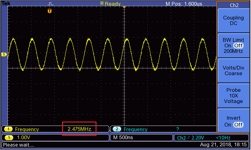
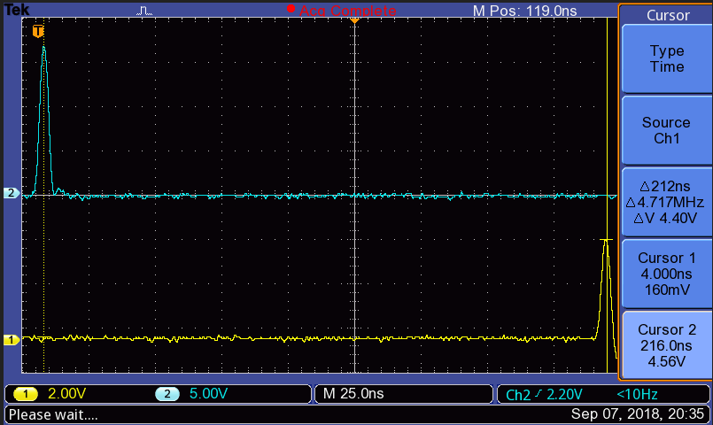
Figure 6. Deterministic Latency Measurement for LMF = 423 ConfigurationThis figure shows the time difference between pulses in the deterministic latency measurement for the LMF = 423 configuration.
9 SCR denotes scrambler. 0 = scrambler disabled; 1 = scrambler enabled.