A.2.2. Function Memory Viewer
Data movement is often a bottleneck in many algorithms. The Function Memory Viewer in the High Level Design Reports (report.html) shows you the memory system that the Intel® HLS Compiler Pro Edition generated for your component. Use the Function Memory Viewer to help you identify data movement bottlenecks in your component design.
Some patterns in memory accesses can cause undesired arbitration in the load-store units (LSUs), which can affect the throughput performance of your component. Use the Function Memory Viewer to find where you might have unwanted arbitration in the LSUs.
Access the Function Memory Viewer by clicking .
The following figure shows the layout of the Function Memory Viewer:
- Function Memory List pane
The Function Memory List pane lists all of the memories in your design. Click a memory name to see its graphical representation in the Function Memory Viewer pane.
- Function Memory Viewer pane
The Function Memory Viewer pane shows a graphical representation of the memory system or memory bank selected in the Function Memory List pane.
- Code view pane
The code view pane shows the source code files for which the reports are generated.
- Details pane
The Details pane shows the details of the memory system or memory bank selected in the Function Memory List pane.
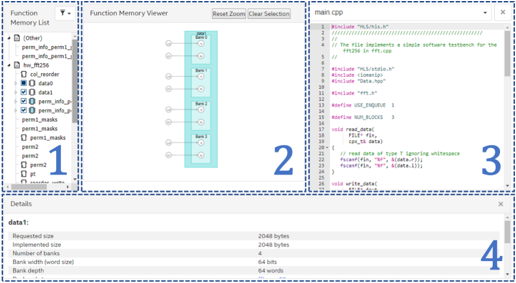
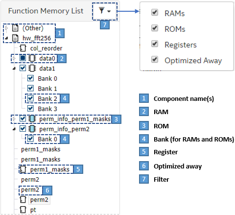
Function Memory List
The Memory List pane shows you a hierarchy of component and task functions, with memories that are synthesized (RAMs, ROMs, and registers) and are optimized away in that component or task.
| Icon or Label | Name | Description | |
|---|---|---|---|
| 1 |  |
Component or task name | The list of memories in your component or task can be expanded or collapsed. Memories that do not belong to any component or task are shown under (Other). |
| 2 |  |
RAM | A RAM is a memory that has at least one write to it. The name of the RAM memory is the same as its name in your design. Clicking the memory name displays a logical representation of the RAM in the Function Memory Viewer pane. By default, only the first bank of the memory system is displayed.To select which banks to display, expand the memory name. Clear the memory name check box to collapse all memory banks in the view. Select the memory name check box to show all memory banks in the view. |
| 3 |  |
ROM | A ROM is a memory that is only read from. The name of the ROM memory is the same as its name in your design. Clicking the memory name displays a logical representation of the ROM in the Function Memory Viewer pane. By default, only the first bank of the memory system is displayed.To select which banks to display, expand the memory name. Clear the memory name check box to collapse all memory banks in the view. Select the memory name check box to show all memory banks in the view. |
| 4 | Bank #num | Bank | A memory bank is always associated with a RAM or a ROM. Each bank is named as Bank #num , where #num is the ID of the memory bank starting from 0. Clicking the bank name shows the bank view in the Function Memory Viewer pane: a graphical representation of the bank, with all of its replicates and private copies. This view can help you to focus on specific memory banks when you view a complex memory design. Clear the memory bank name check box to collapse the bank in the logical representation of the memory. Select the memory bank name check box to show the bank in the logical representation of the memory. |
| 5 |  |
Register | A register is a component variable that is carried through the pipeline in registers rather than being stored in a RAM or ROM. The name of the register is the same as its name in your design. A register variable can be implemented either exclusively in flip-flops (FFs), or in a mix of FFs and RAM-based FIFOs. |
| 6 | text label | Optimized Away | A component variable might be optimized away because it is unused in your design or compiler optimizations have transformed all uses of the variable such that it is unnecessary. The name of the optimized away variable is the same as its name in your design. |
| 7 |  |
Filter | Use the Function Memory List filter to selectively view the list of RAMs, ROMs, registers and optimized away variables in your design. Clearing the check box associated with a item in the filter hides all occurrences of that kind of item in the Function Memory List. Filter your Function Memory List to help you focus on a specific type of memory in your design. |
Function Memory Viewer
The Function Memory Viewer pane shows you connections between loads and stores to specific logical ports on the banks in a memory system. It also shows you the number of replicates and private copies created per bank for your memory system. The following types of nodes might be shown in the Function Memory Viewer pane, depending on the component memory system and what you have selected in the Function Memory List pane:
- Memory node: The memory system for a given variable in your design.
- Bank node: A bank in the memory system. A memory system contains at least one memory bank. A memory bank can have one or more port nodes. Only banks selected in the Function Memory List pane are shown.
- Replication node: A replication node shows memory bank replicates that are created to efficiently support multiple accesses to a local memory. A bank contains at least one replicate. You can view replicate nodes only when you view a memory bank by clicking its name in the Function Memory List pane.
- Private-copy node: A private-copy node shows private copies within a replicate that are created to allow concurrent execution of multiple loop iterations. A replicate contains at least one private copy. You can view private-copy nodes only when you view a memory bank by clicking its name in the Function Memory List pane
- Port node: Each read or write access to a local memory is mapped to a port. There are three types of port:
- R: A read-only port
- W: A write-only port
- RW: A read and write port
- LSU node: A store (ST) or load (LD) node connected to the memory through port nodes.
- Arbitration node: An arbitration (ARB) node shows that LSUs compete for access to a shared port node, which can lead to stalls.
- Port-sharing node: A port-sharing node (SHARE) shows that LSUs have mutually exclusive access to a shared port node, so the load-store units are free from stalls.
Hover over any node to view the attributes of that node.
Hover over an LSU node to highlight the path from the LSU node to all of the ports that the LSU connects to.
Hover over a port node to highlight the path from the port node to all of the LSUs that read or write to the port node.
Click a node to select it and have the node attributes displayed in the Details pane.
Code View
The code view pane shows your source code.
Clicking on a memory or a bank in the Function Memory Viewer pane highlights the line of your code (in the code view pane) where you declared the memory.
Clicking on a load or store node in the Function Memory Viewer pane highlights the line of your code (in the code view pane) where you read from or write to memory.
Details
The Details pane shows the attributes of the node selected in the Function Memory Viewer pane. For example, when you select a memory in a component, the Details pane shows information such as the width and depths of the memory banks, the memory layout information, the address bit mapping and any user-defined HLS attributes that you specified in your source code.
For an example of this difference, see Example: Specifying Bank-Selection Bits for Local Memory Addresses in the Intel® HLS Compiler Pro Edition Best Practices Guide .
The content of the Details pane persists until you select a different node in the Component/Function Memory Viewer pane.