Intel® High Level Synthesis Compiler Pro Edition: Best Practices Guide
8.4. Example: Specifying Bank-Selection Bits for Local Memory Addresses
The (b 0 , b 1 , ... ,b n ) arguments refer to the local memory address bit positions that the Intel® HLS Compiler Pro Edition should use for the bank-selection bits. Specifying the hls_bankbits(b 0, b 1 , ..., b n) attribute implies that the number of banks equals 2 number of bank bits .
| Bank 0 | Bank 1 | Bank 2 | Bank 3 | |
| Word 0 | 00 000 | 01 000 | 10 000 | 11 000 |
| Word 1 | 00 001 | 01 001 | 10 001 | 11 001 |
| Word 2 | 00 010 | 01 010 | 10 010 | 11 010 |
| Word 3 | 00 011 | 01 011 | 10 011 | 11 011 |
| Word 4 | 00 100 | 01 100 | 10 100 | 11 100 |
| Word 5 | 00 101 | 01 101 | 10 101 | 11 101 |
| Word 6 | 00 110 | 01 110 | 10 110 | 11 110 |
| Word 7 | 00 111 | 01 111 | 10 111 | 11 111 |
Example of Implementing the hls_bankbits Attribute
component int bank_arbitration (int raddr,
                                int waddr,
                                int wdata) {

  #define DIM_SIZE 4

  // Adjust memory geometry by preventing coalescing
  hls_numbanks(1)
  hls_bankwidth(sizeof(int)*DIM_SIZE)

  // Force each memory bank to have 2 ports for read/write
  hls_singlepump
  hls_max_replicates(1)

  int a[DIM_SIZE][DIM_SIZE][DIM_SIZE];
  // initialize array a…
  int result = 0;

  #pragma unroll
  for (int dim1 = 0; dim1 < DIM_SIZE; dim1++)
    #pragma unroll
    for (int dim3 = 0; dim3 < DIM_SIZE; dim3++)
      a[dim1][waddr&(DIM_SIZE-1)][dim3] = wdata;

  #pragma unroll
  for (int dim1 = 0; dim1 < DIM_SIZE; dim1++)
    #pragma unroll
    for (int dim3 = 0; dim3 < DIM_SIZE; dim3++)
      result += a[dim1][raddr&(DIM_SIZE-1)][dim3];

  return result;
}
As illustrated in the following figure, this code example generates multiple load and store instructions, and therefore multiple load/store units (LSUs) in the hardware. If the memory system is not split into multiple banks, there are fewer ports than memory access instructions, leading to arbitrated accesses. This arbitration results in a high loop initiation interval (II) value. Avoid arbitration whenever possible because it increases the FPGA area utilization of your component and impairs the performance of your component.
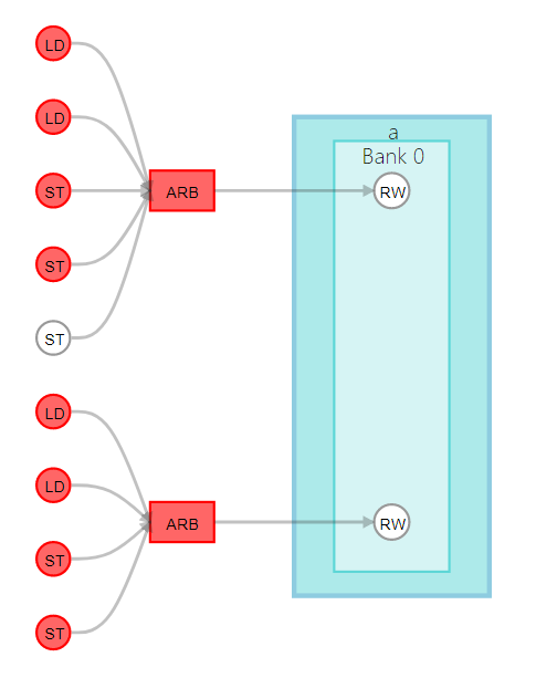
By default, the Intel® HLS Compiler Pro Edition splits the memory into banks if it determines that the split is beneficial to the performance of your component. The compiler checks if any bits remain constant between accesses, and automatically infers bank-selection bits.
component int bank_no_arbitration (int raddr,
                                   int waddr,
                                   int wdata) {
  #define DIM_SIZE 4

  // Adjust memory geometry by preventing coalescing and splitting memory
  hls_bankbits(4, 5)
  hls_bankwidth(sizeof(int)*DIM_SIZE)

  // Force each memory bank to have 2 ports for read/write
  hls_singlepump
  hls_max_replicates(1)

  int a[DIM_SIZE][DIM_SIZE][DIM_SIZE];

  // initialize array a…
  int result = 0;

  #pragma unroll
  for (int dim1 = 0; dim1 < DIM_SIZE; dim1++)
    #pragma unroll
    for (int dim3 = 0; dim3 < DIM_SIZE; dim3++)
      a[dim1][waddr&(DIM_SIZE-1)][dim3] = wdata;

  #pragma unroll
  for (int dim1 = 0; dim1 < DIM_SIZE; dim1++)
    #pragma unroll
    for (int dim3 = 0; dim3 < DIM_SIZE; dim3++)
      result += a[dim1][raddr&(DIM_SIZE-1)][dim3];

  return result;
}
The following diagram shows that this example code creates a memory configuration with four banks. Using bits 4 and 5 as bank selection bits ensures that each load/store access is directed to its own memory bank.
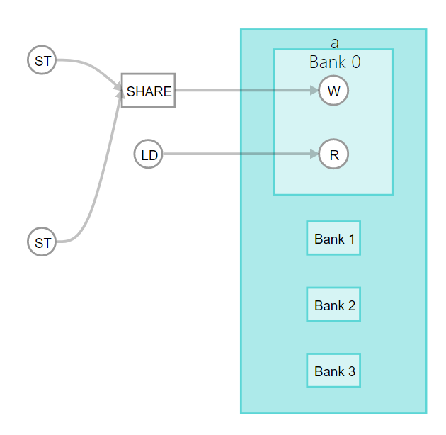
In this code example, setting hls_numbanks(4) instead of hls_bankbits(4,5) results in the same memory configuration because the Intel® HLS Compiler Pro Edition automatically infers the optimal bank selection bits.
In the Function Memory Viewer (inf the High-Level Design Reports), the Address bit information shows the bank selection bits as b6 and b7, instead of b4 and b5:
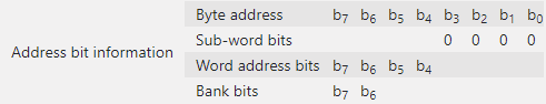
This difference occurs because the address bits reported in the Function Memory Viewer are based on byte addresses and not element addresses. Because every element in array a is four bytes in size, bits b4 and b5 in element address bits correspond to bits b6 and b7 in byte addressing.