1.7. Pin Placement for Intel® Stratix® 10 EMIF IP
Overview
- Each device contains between 2 and 3 I/O columns.
- Each I/O column contains up to 12 I/O banks.
- Each I/O bank contains 4 lanes.
- Each lane contains 12 general-purpose I/O (GPIO) pins.
General Pin Guidelines
The following points provide general pin guidelines:
- Ensure that the pins for a given external memory interface reside within a single I/O column.
- Interfaces that span multiple banks must meet the following requirements:
- The banks must be adjacent to one another. For information on adjacent banks, refer to the Intel Stratix 10 External Memory Interfaces IP User Guide.
- The address and command bank must reside in a center bank to minimize latency. If the memory interface uses an even number of banks, the address and command bank may reside in either of the two center banks.
- Unused pins can be used as general-purpose I/O pins.
- All address and command and associated pins must reside within a single bank.
- Address and command and data pins can share a bank under the following conditions:
- Address and command and data pins cannot share an I/O lane.
- Only an unused I/O lane in the address and command bank can be used for data pins.
| Signal Type | Constraint |
|---|---|
| Data Strobe | All signals belonging to a DQ group must reside in the same I/O lane. |
| Data | Related DQ pins must reside in the same I/O lane. For protocols that do not support bidirectional data lines, read signals should be grouped separately from write signals. |
| Address and Command | Address and Command pins must reside in predefined locations within an I/O bank. |
Adjacent Banks
For banks to be considered adjacent, they must reside in the same I/O column, To determine if banks are adjacent, refer to the Modular I/O banks Location and Pin Counts in Stratix 10 Devices section located in the Stratix 10 General Purpose I/O User Guide.
When referring to tables in the Stratix 10 General Purpose I/O User Guide, it is safe to assume that all banks shown are adjacent, unless a ' - ' symbol is present; a ' - ' symbol indicates that the bank is not bonded out for the package.
Pin Assignments
To determine locations for all EMIF I/O pins you should reference the pin table for your device. When referring to the pin table, the bank numbers, I/O bank indices, and pin names are provided. You can find the pin indices for address and command pins in the Stratix 10 Scheme Table located on the Intel® FPGA website.
You can perform pin assignments in a variety of ways. The recommended approach is to manually constrain some interface signals and let the Intel® Quartus® Prime Fitter handle the rest. This method consists of consulting the pin tables to find legal positions for some of the interface pins and assigning them through the .qsf file that is generated with the EMIF design example. For this method of I/O placement, you must constrain the following signals:
- CK0
- One DQS pin per group
- PLL reference clock
- RZQ
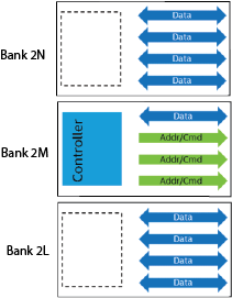
Based on the above constraints, the Intel® Quartus® Prime Fitter rotates pins within each lane as necessary. The following figure illustrates an example of pin assignments for a DDR3 x72 interface with the following selections:
- The address and command pin is placed in bank 2M and requires 3 lanes.
- CK0 is constrained to pin 8 in bank 2M.
- PLL reference clock pins are constrained to pins 24 and 25 in bank 2M.
- RZQ is constrained to pin 26 in bank 2M.
- Data is placed in banks 2N, 2M, and 2L, and requires 9 lanes.
- DQS groups 1-4 are placed in bank 2N.
- DQS group 0 is placed in bank 2M.
- DQS groups 5-8 are placed in bank 2L.
In this example, to constrain CK0 to pin 8 in bank 2M, you would add the following line to the .qsf file, based on the appropriate pin table:
set_location_assignment PIN_K31 -to CK0
The format of the above pin assignment can be applied to all pins:
set_location_assignment <pin name> -to <signal name>