F-Tile Avalon® Streaming Intel® FPGA IP for PCI Express* Design Example User Guide
ID
683372
Date
10/04/2022
Public
A newer version of this document is available. Customers should click here to go to the newest version.
3.7.3. Running the Performance Design Example
Note: The Performance Design Example hardware test is currently supported at 500 MHz only.
- Navigate to ./software/user/example under the design example directory.
- Compile the design example application:
$ make -
Run the test:
$ sudo ./intel_fpga_pcie_link_testYou can run the Intel FPGA IP PCIe link test application in manual or automatic mode. Select from:- In automatic mode, the application automatically selects the device. The test selects the Intel PCIe device with the lowest BDF by matching the Vendor ID. The test also selects the lowest available BAR.
- In manual mode, the test queries you for the bus, device, and function number and BAR.
For the Intel Agilex Development Kit, you can determine the BDF by typing the following command:$ lspci -d 1172: - Here are sample transcripts for automatic and manual modes:
Figure 31. Automatic Mode
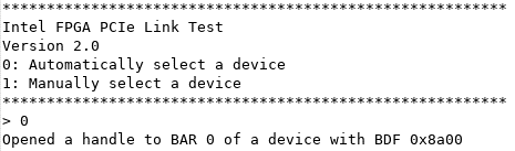 Figure 32. Manual Mode
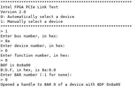
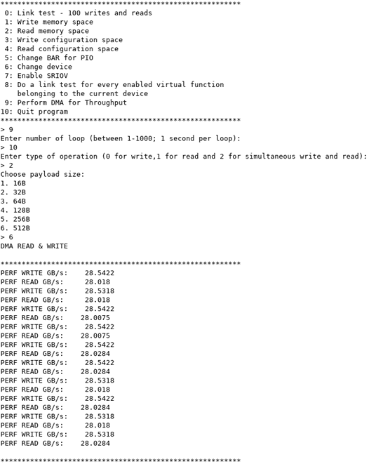
- To perform DMA for throughput test, enter option “9” and press Enter key to proceed.
- Enter number of DMA iterations to be carried out and then press Enter key to select the type of DMA operation, “0” for write operation (device to host), “1” for read operation (host to device) and “2” for simultaneous write and read operations.
- Select payload size for the TLPs used for the throughput test.
Here are block diagrams and sample test results for write only, read only and simultaneous write and read for 10 iterations respectively.
Figure 33. Write Only Operation
Figure 34. Write Only Test Result
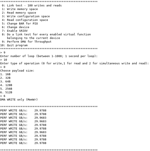
Figure 35. Read Only Operation
Figure 36. Read Only Test Result
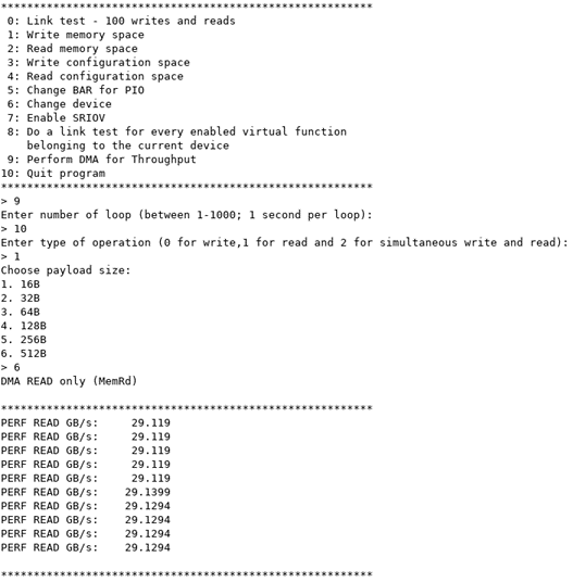
Figure 37. Simultaneous Write and Read Operation
Figure 38. Simultaneous Write and Read Test Result
Performance Design Example Data Throughput
The following test result is obtained using the hardware and software as mentioned in Hardware and Software Requirements.
The data throughput values may vary especially when a different host system is used.
| TLP Payload Size (Byte) | Data Throughput | |||
|---|---|---|---|---|
| Memory Write (GB/s) | Memory Read (GB/s) | Simultaneous Write and Read | ||
| Write (GB/s) | Read (GB/s) | |||
| 64 | 22.80 | 21.08 | 17.86 | 17.63 |
| 128 | 26.40 | 25.67 | 22.72 | 22.38 |
| 256 | 28.69 | 27.85 | 26.31 | 25.88 |
| 512 | 29.97 | 29.12 | 28.02 | 28.54 |
Note: Data throughput at 16 and 32 bytes TLP payload size does not meet expected throughput values. It may be addressed in the future Intel® Quartus® Prime software release.