4.4. Cyclone® 10 GX EPE - RAM Worksheet
Each row in the RAM worksheet of the EPE spreadsheet represents a logical RAM module that can be implemented using one or more physical RAM blocks. The EPE spreadsheet implements each logical RAM module with the minimum number of physical RAM blocks, in the most power-efficient way possible, based on the specified logical width and depth.
You must know how your RAM is implemented by the Quartus® Prime Compiler when you are selecting the RAM block mode. For example, if a ROM is implemented with two ports, it is considered a true dual-port memory and not a ROM. Single-port and ROM implementations use only one port. Simple dual-port and true dual-port implementations use both Port A and Port B.
- The Early Power Estimator reports MLAB power in the RAM worksheet. However the Power Analyzer reports MLAB power as Combinational cell and Register cell block type in the Thermal Power Dissipation by Block Type section of the power report.
- The Power Analyzer reports LAB clock power as Block Thermal Dynamic Power under Clock Network block type in the Thermal Power Dissipation by Block Type section of the power report. The Early Power Estimator reports LAB clock power in either the Clock or RAM worksheet, depending on whether the LAB is used to implement logic or used as MLAB, respectively.
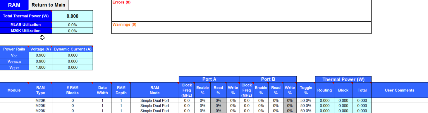
| Column Heading | Description |
|---|---|
| Module | Enter a name for the RAM module in this row. This is an optional value. |
| RAM Type | Select the implemented RAM type. You can find the RAM type in the Type column of the Quartus Prime Compilation Report. In the Compilation Report, select Fitter and click Resource Section. Click Fitter RAM Summary. |
| # RAM Blocks | Enter the number of RAM blocks in the module that use the same type and mode and have the same parameter for each port. The parameters for each port are as follows:
You can find the number of RAM blocks in either the MLAB cells or M20K blocks column of the Quartus Prime Compilation Report. In the Compilation Report, select Fitter and click Resource Section. Click Fitter RAM Summary. |
| Data Width | Enter the width of the data for the RAM block. This value is limited based on the RAM type. You can find the width of the RAM block in the Port A Width or the Port B Width column of the Quartus Prime Compilation Report. In the Compilation Report, select Fitter and click Resource Section. Click Fitter RAM Summary. For RAM blocks that have different widths for Port A and Port B, use the larger of the two widths. |
| RAM Depth | Enter the depth of the RAM block in number of words. You can find the depth of the RAM block in the Port A Depth or the Port B Depth column of the Quartus Prime Compilation Report. In the Compilation Report, select Fitter and click Resource Section. ClickFitter RAM Summary. |
| RAM Mode | Select from the following modes:
The mode is based on how the Quartus Prime Compiler implements the RAM. If you are unsure how your memory module is implemented, Intel recommends compiling a test case in the required configuration in the Quartus Prime software. You can find the RAM mode in the Mode column of the Quartus Prime Compilation Report. In the Compilation Report, select Fitter and click Resource Section. Click Fitter RAM Summary. A single-port RAM has one port with a read and a write control signal. A simple dual-port RAM has one read port and one write port. A true dual-port RAM has two ports, each with a read and a write control signal. ROMs are read-only single-port RAMs. |
| Port A - Clock Freq (MHz) | Enter the clock frequency for Port A of the RAM blocks (in MHz). This value is limited by the maximum frequency specification for the RAM type and device family. |
| Port A - Enable % | The average percentage of time the Port A clock enable is active, regardless of activity on RAM data and address inputs. This number must be a percentage between 0% and 100%. RAM power is primarily consumed when a clock event occurs. Using a clock enable signal to disable a port when no read or write operation is occurring can result in significant power savings. |
| Port A - Read % | Enter the percentage of time Port A of the RAM block is in read mode. This field is applicable only for single port and true dual port RAMs. This value must be a percentage number between 0 and 100%. |
| Port A - Write % | Enter the average percentage of time Port A of the RAM block is in write mode. This field is applicable only for single port, dual port and true dual port RAMs. This value must be a percentage number between 0 and 100%. |
| Port B - Clock Freq (MHz) | Enter the clock frequency for Port B of the RAM blocks (in MHz). |
| Port B - Enable % | Enter the average percentage of time the input clock enable for Port B is active, regardless of the activity on the RAM data and address inputs. The enable percentage ranges from 0 to 100%. RAM power is primarily consumed when a clock event occurs. Using a clock-enable signal to disable a port when no read or write operation is occurring can result in significant power savings. |
| Port B - Read % | Enter the percentage of time Port B of the RAM block is in read mode. This field is applicable only to dual port and true dual port RAMs and ROMs. This value must be a percentage number between 0 and 100%. |
| Port B - Write % | Enter the percentage of time Port B of the RAM block is in write mode. This field is only available for true dual-port mode. This value must be a percentage number between 0 and 100%. |
| Toggle % | The percentage of clock cycles when the block output signal changes value. This value is multiplied by the clock frequency and the enable percentage to determine the number of transitions per second. This value affects only routing power. 50% corresponds to a randomly changing signal, since half the time the signal will hold the same value and thus not transition. This is considered the highest meaningful toggle rate for a RAM block. |
| Thermal Power (W) - Routing | Indicates the power dissipation due to estimated routing (in W). Routing power depends on placement and routing, which is a function of design complexity. The values shown represent the routing power estimate based on observed behavior across more than 100 real-world designs. Use the Quartus Prime Power Analyzer for accurate analysis based on the exact routing used in your design. |
| Thermal Power (W) - Block | Indicates the power dissipation due to internal toggling of the RAM (in W). Use the Quartus Prime Power Analyzer for accurate analysis based on the exact RAM modes in your design. |
| Thermal Power (W) - Total | Indicates the estimated power (in W), based on information entered into the EPE spreadsheet. Total power is equal to the sum of routing power and block power. |
| User Comments | Enter any comments. This is an optional entry. |