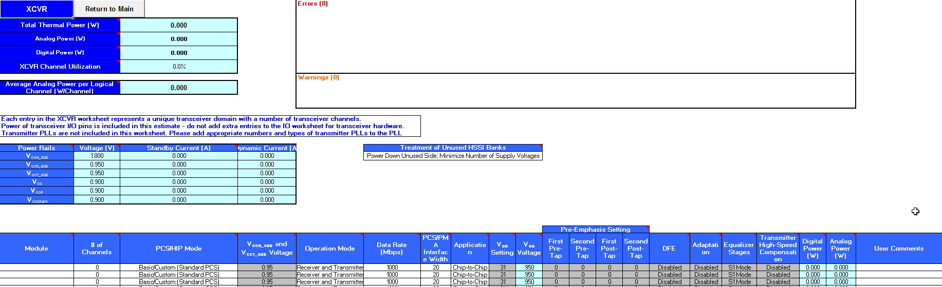
4.10. Cyclone® 10 GX EPE - XCVR Worksheet
The Early Power Estimator does not include power estimates for the On-Die Instrumentation (ODI) XCVR block. To estimate power for transceiver channels that include the ODI block, use the Quartus® Prime Power Analyzer.
The Early Power Estimator makes the following simplifying assumptions about the transceiver clock network and the blocks used:
- x6 clock lines are used for all GX channels. (Refer to the Cyclone® 10 GX Transceiver PHY User Guide for details on the clock line types.)
- For each duplex (both receiver and transmitter active) and transmitter-only row in the XCVR worksheet, there is one master CGB and one reference clock pin per 6 channels. Each row has at least one master CGB and at least one reference clock pin. Rows with receiver-only channels assume there is one reference clock pin per 6 channels, but no master CGBs. Each row has at least one reference clock pin.
For example, a single-channel duplex design assumes one master CGB and one reference clock pin. The same is true if 6 channels are entered on one row. However, if 6 channels are entered into 6 rows (1 channel per row), each row assumes one master CGB and one reference clock pin, for a total of six master CGBs and six reference clock pins. Consequently, entering the same number of identical channels into individual rows results in a slightly different power estimate than if all channels are entered into one row.
| Input Parameter | Description |
|---|---|
| Treatment of Unused HSSI Banks | Specifies how transceiver banks not actively used by channels should be treated when calculating static power. You can select one of the following options:
If all high-speed serial interface (HSSI) banks on one side are not used, they can all be powered down or remain powered up. You can select the voltage for unused-but-powered banks to minimize static power (that is, leakage), or to minimize the number of power supply voltages required. For example, if active transceiver channels use VCCR_GXB=1.03V, selecting Minimize Leakage will assume the unused-but-powered banks use VCCR_GXB=0.95V, which is the lowest supported voltage (assuming that the currently selected device supports this voltage). Selecting Minimize Number of Supply Voltages will assume the unused-but-powered banks use VCCR_GXB=1.03V, which is the lowest voltage used by active channels, thus eliminating the need for the 0.95V power supply on VCCR_GXB.
If you select Power Down Unused Side, unused HSSI banks on the side that has active channels are still powered. This is because HSSI banks cannot be powered down individually; only the whole HSSI side can be powered down. For more details, refer to the Cyclone® 10 GX Device Family Pin Connection Guidelines.
Note: PLLs specified in the PLL worksheet, and their VCCR_GXB voltages, are also considered when determining how many HSSI banks are actively used. For example, if all active channels in the XCVR worksheet use VCCR_GXB=1.03V, but one PLL in the PLL worksheet uses VCCR_GXB=0.95V, there will be at least one HSSI bank operating at VCCR_GXB=0.95V.
|
Each row in the XCVR worksheet represents a separate transceiver domain. Enter the following parameters for each transceiver domain:
| Column Heading | Description |
|---|---|
| Module | Specifies a name for the module. This is an optional value. |
| # of Channels | Specifies the number of channels used in this transceiver domain. Each row represents one transceiver domain. These channels are grouped together in one transceiver bank, or two or more adjacent transceiver banks and clocked by one or more common transmitter PLLs.
Note: For PCI Express protocols with Hard IP, the Hard IP block supports x1, x2, and x4 modes.
|
| PCS/HIP Mode | Specifies the mode in which the PCS and HIP blocks operate. This mode depends on the communication protocol or standard that the channels on this row implement. |
| VCCR_GXB and VCCT_GXB Voltage | Specifies the voltage of the VCCR_GXB and VCCT_GXB rails. Allowed values depend on the selected device and selected data rate. |
| Operation Mode | Specifies whether the hardware is configured in full duplex transceiver mode (Receiver and Transmitter) or in Receiver Only or Transmitter Only mode. Allowed values depend on the selected PCS/HIP mode. |
| Data Rate (Mbps) | Specifies the data rate (in Mbps) for the transceiver. Allowed values depend on the selected protocol, selected device, and the VCCR_GXB and VCCT_GXB voltages. |
| PCS/PMA Interface Width | Specify the width of the parallel data bus between PCS and PMA. |
| Application | Select the application type from Chip-to-Chip, Backplane, or Custom. Select Custom to enable manual editing of advanced channel options for the current row. |
| VOD Setting | The output differential voltage (VOD) setting of the transmitter channel PMA. To enable this setting, select Custom in the Application column. |
| VOD Voltage | The output differential voltage (VOD) of the transmitter channel PMA (in mV). This voltage depends on the VOD setting and the VCCT_GXB voltage. For the purpose of power calculation, it is assumed that the transmitter uses a termination resistance of 100 Ohms. |
| Pre-Emphasis Setting–First Pre-Tap | Specifies the pre-emphasis setting used by the transmitter channel PMA. Allowed values for individual taps depend on selected VOD setting and selected values of other pre-emphasis taps. Only positive values of tap settings are listed. Power consumption does not depend on the sign (positive or negative) of individual taps. To enable these settings, select Custom in the Application column. |
| Pre-Emphasis Setting–Second Pre-Tap | |
| Pre-Emphasis Setting–First Post-Tap | |
| Pre-Emphasis Setting–Second Post-Tap | |
| DFE | Specify mode of the decision feedback equalizer (DFE). Allowed values depend on the selected data rate. To enable this setting, select Custom in the Application column. |
| Adaptation | Specify if the adaptation feature is used. This option should be enabled if the channels use either CTLE adaptation or DFE adaptation. To enable this setting, select Custom in the Application column. |
| Equalizer Stages | Specify whether the continuous time linear equalizer (CTLE) uses high data rate mode (S1 Mode) or high gain mode (Non-S1 Mode). Allowed values depend on the selected data rate. To enable this setting, select Custom in the Application column. |
| Transmitter High-Speed Compensation | Specifies if the power distribution network (PDN) induced inter-symbol interference (ISI) compensation is enabled in the TX driver. To enable this setting, select Custom in the Application column. |
| Digital Power (W) | The total power of the transmitter channel PCS, receiver channel PCS, and PCI Express Hard IP blocks used by all channels on this row (in W). |
| Analog Power (W) | The total power of all analog circuitry on this row (in W). This power excludes power of PCS and PCI Express Hard IP blocks, whose power is provided in the Digital Power column, and transmitter PLLs, whose power is provided in the PLL worksheet. |
| User Comments | Enter any comments. This is an optional entry. |
For more information about the transceiver architecture of the supported device families, refer to the Transceiver PHY User Guide for Cyclone® 10 GX.