AN 905: JESD204B Intel® FPGA IP and ADI AD9213 Interoperability Report for Intel Stratix® 10 Devices
1.2. Hardware Setup
An Intel® Stratix® 10 GX Signal Integrity Development Kit is used with the ADI AD9213 daughter card module installed to the development board’s FMC+ connector.
- The AD9213 EVM derives power from the FMC+ pins.
- The FPGA clock is supplied by a Silicon Labs Si5341 clock generator on the development kit.
- The Si5341 clock generator provides a reference clock to the ADF4355 clock source. Sampling clock to the ADC AD9213 EVM is given by external clock source ADF 4355.
- For subclass 1, the FPGA generates SYSREF for the JESD204B Intel® FPGA IP as well as the AD9213 device.
- SYSREF is provided to ADC through SMA connector.
Figure 1. Hardware Setup
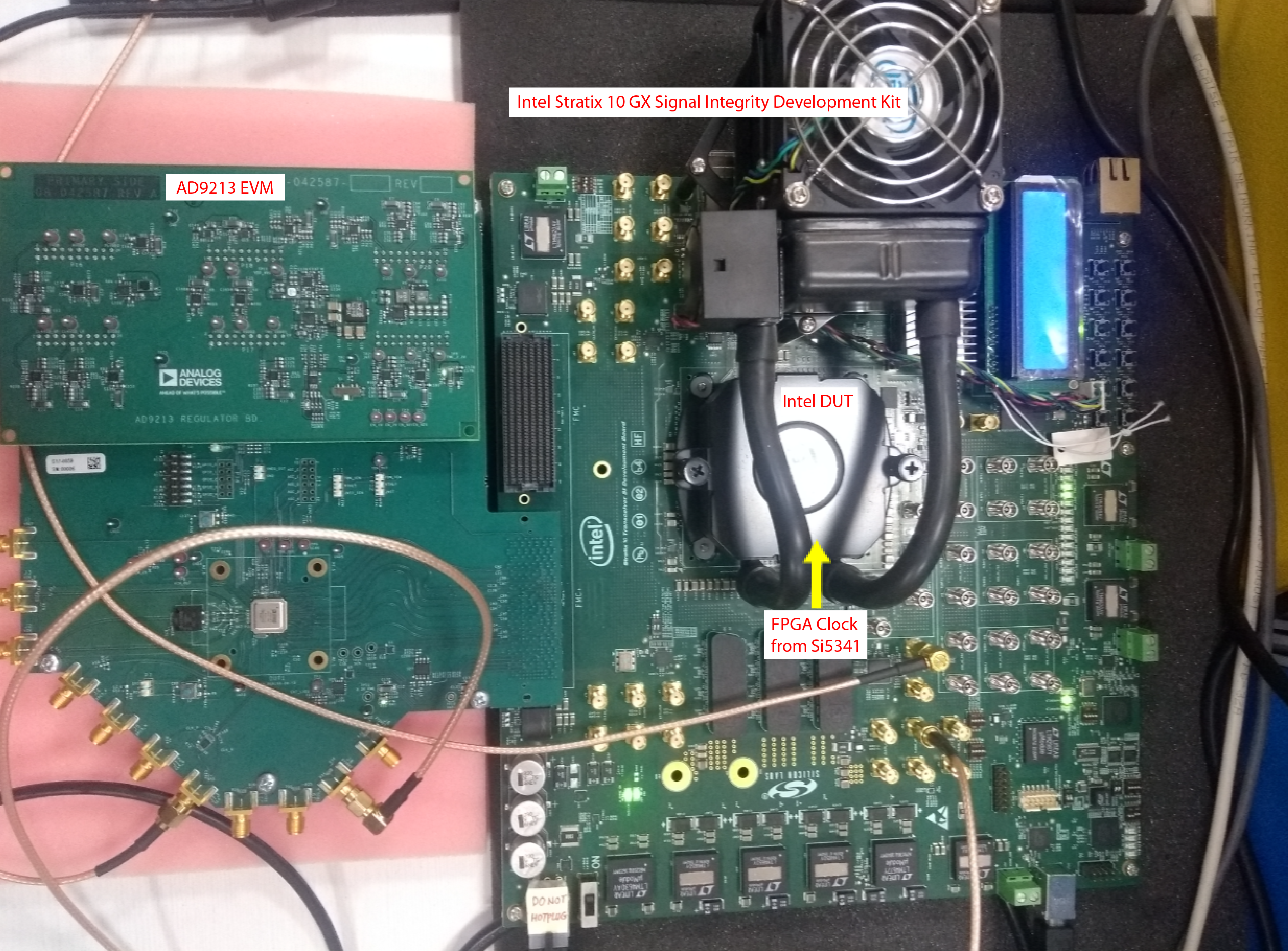
Figure 2. System DiagramThis system-level diagram shows how the different modules connect.
In this setup, where LMF = 812, the data rate of the transceiver lanes is 16 Gbps. An external clock source card provides 400 MHz clock to the FPGA and 6400 MHz sampling clock to AD9213 device. A periodic SYSREF is generated by the FPGA and provided to the ADC through the SMA connector. The JESD204B Intel® FPGA IP core is instantiated in duplex mode but only the receiver path is used.