A newer version of this document is available. Customers should click here to go to the newest version.
6.4. Top Level
The top-level Verilog file and HPS configuration is derived directly from the GSRD designs located at RocketBoards.org. For more information about the Intel® Arria® 10 SoC GSRD, refer to the following URL: https://www.rocketboards.org/foswiki/Documentation/arria10SoCGSRD
The GSRD designs have been modified to include the Intel® FPGA AI Suite IP. All unnecessary logic has been removed, which provides a concise design example.
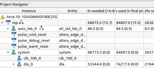
The main Intel® FPGA AI Suite SoC design example is contained within a single Platform Designer system, called system. Double-click this node in the Intel® Quartus® Prime Project Navigator to launch Platform Designer.