Power Rail Inputs
Refer to the Pin Connection Guidelines for your selected Intel FPGA to determine what inputs you can group together; the Pin Connection Guidelines recommend a power supply block architecture for each FPGA configuration and provide details about each input pin required during hardware design.
Intel suggests power rail groupings in the Pin Connection Guidelines for each Intel FPGA, but there are two other factors to consider when grouping your power rails. First, each of the FPGA power rail inputs in a group must have the same supply voltage requirement. This limitation is important for FPGA resource blocks such as I/O inputs that might require different voltages depending on the specific interface protocols used in your design. For example, a PCI Express® ( PCIe® ) I/O interface might require a 3 V input supply and an LVDS I/O interface might require a 2.5 V input supply; while both are I/O inputs, and the Pin Connection Guidelines simplified the I/O inputs as a single VCCIO rail, these two I/O inputs must be powered by different converters.
The second power rail grouping factor to consider is power-up sequencing. Not every FPGA or system requires power-up sequencing, but many advanced FPGAs require that power is supplied to various inputs in a specific order during system power-up. You can locate the power-up sequence guidelines for your selected Intel FPGA in the device’s Pin Connection Guidelines or Handbook. If your design requires power-up sequencing, you must ensure that grouped power rail inputs meet the sequence requirements for your Intel FPGA. You cannot provide power to a power rail if it depends upon another rail in the same group or a rail in a later group.
You can provide power to any inputs in your design individually, or in combination with another group of FPGA inputs that share their voltage and sequencing requirements.
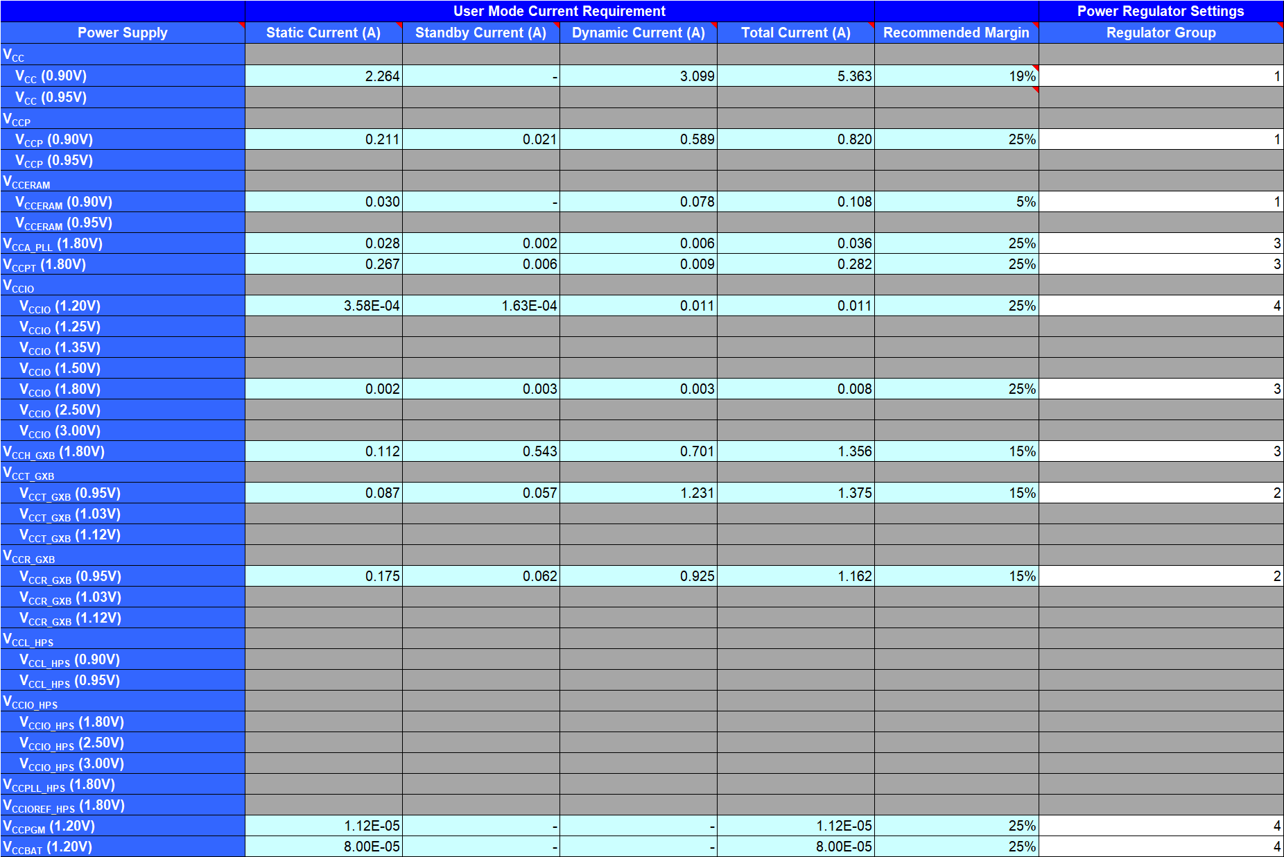
Once you determine your power rail input groupings, use the Early Power Estimator (EPE) spreadsheet to determine the total power required for the input group. The EPE spreadsheet combines the current requirements for each load by summing each FPGA input’s current requirement. The result are in in the Total Current (A) column in the EPE spreadsheet Report tab.
In the EPE spreadsheet you can group inputs at any point in your design cycle, including before you start your design, or before your design is complete.