A newer version of this document is available. Customers should click here to go to the newest version.
1. Answers to Top FAQs
2. Overview of the Intel® FPGA Power and Thermal Calculator
3. Estimating Power Consumption with the Intel® FPGA Power and Thermal Calculator
4. Intel® FPGA Power and Thermal Calculator Graphical User Interface
5. Intel® FPGA Power and Thermal Calculator Pages
6. Factors Affecting the Accuracy of the Intel® FPGA PTC
7. Intel® FPGA Power and Thermal Calculator User Guide Archive
8. Document Revision History for the Intel® FPGA Power and Thermal Calculator User Guide
A. Measuring Static Power
5.1. Intel® FPGA PTC - Power Summary
5.2. Intel® FPGA PTC - Common Page Elements
5.3. Intel® FPGA PTC - Main Page
5.4. Intel® FPGA PTC - Logic Page
5.5. Intel® FPGA PTC - RAM Page
5.6. Intel® FPGA PTC - DSP Page
5.7. Intel® FPGA PTC - Clock Page
5.8. Intel® FPGA PTC - PLL Page
5.9. Intel® FPGA PTC - I/O Page
5.10. Intel® FPGA PTC - Transceiver Page
5.11. Intel® FPGA PTC - HPS Page
5.12. Intel® FPGA PTC - Crypto Page
5.13. Intel® FPGA PTC - HBM Page
5.14. Intel® FPGA PTC - Thermal Page
5.15. Intel® FPGA PTC - Report Page
5.8. Intel® FPGA PTC - PLL Page
Each row in the PLL data entry page of the Intel® FPGA Power and Thermal Calculator (PTC) represents one or more PLLs in the device.
Supported PLL types are family dependent, as outlined in the PLL Page Information table, below.
| Column Header | Description |
|---|---|
| Total thermal power (W) | Reports the total thermal power (in W). |
| fPLL utilization | Reports the percentage of fPLL utilization. (This field is available for Intel® Stratix® 10 devices only.) |
| IO PLL utilization | Reports the percentage of I/O PLL utilization. |
| ATX PLL utilization | Reports the percentage of ATX PLL utilization. (This field is available for Intel® Stratix® 10 devices only.) |
| CMU/CDR PLL utilization | Reports the percentage of CMU/CDR PLL utilization. (This field is available for Intel® Stratix® 10 devices only.) |
| Power rails | Indicated the voltage (mV), dynamic current (A), and standby current (A), for various power rails. |
Figure 30. PLL Page
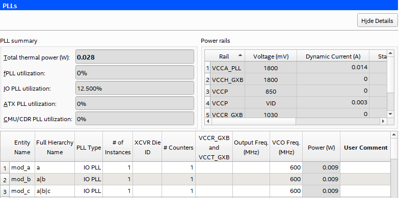
| Column Heading | Description |
|---|---|
| Entity Name | Specify a name for the PLL entity in this column. This is an optional value. |
| Full Hierarchy Name | Specify the hierarchical path relevant to this entry. This is an optional entry. When entering levels of hierarchy, the pipe character (|) denotes a level of hierarchy. |
| PLL Type | Specifies the type of PLL, which may include the following:
|
| # of Instances | The number of logical PLL instances with this type, counter, voltage, and frequency combination. |
| Bank ID | The I/O bank ID for this row. A bank location can be assigned to PLLs to change how the PLLs are placed, affecting thermals and utilization. (This column is available for Intel® Agilex™ devices only.) |
| # PLL Blocks | Enter the number of PLL blocks with the same combination of parameters. |
| XCVR Die ID | Specify the transceiver die on which PLLs on this row are located. This field is not applicable for I/O PLLs, nor fabric-feeding I/O PLLs. |
| # Counters | Enter the number of counters of the PLL. |
| VCCR_GXB and VCCT_GXB Voltage | Specify the voltage of the VCCR_GXB and VCCT_GXB rails. This field is not applicable for I/O PLLs, nor fabric-feeding I/O PLLs. |
| Output Freq (MHz) | Specify the output frequency for CMU and ATX PLLs. |
| VCO Freq (MHz) | Specify the internal VCO operating frequency for PLLs. |
| Total Power (W) | Shows the total estimated power for this row (in W). |
| User Comments | Enter any comments. This is an optional entry. |
For more information about the PLLs available in Intel® Agilex™ devices, refer to the Intel® Agilex™ Clocking and PLL User Guide.
Related Information