3.8.3. NCO IP Core Timing Diagrams
All NCO architectures, except for serial CORDIC and multi-cycle multiplier-based architectures, output a sample every clock cycle. After the clock enable is asserted, the oscillator outputs the sinusoidal samples at a rate of one sample per clock cycle, following an initial latency of L clock cycles. The exact value of L varies across architectures and parameterizations.
After the clock enable is asserted, the oscillator outputs the sinusoidal samples at a rate of one sample for every two clock cycles, following an initial latency of L clock cycles. The exact value of L depends on the parameters that you set.
After the clock enable is asserted, the oscillator outputs sinusoidal samples at a rate of one sample per N clock cycles, where N is the magnitude precision. The IP core has an initial latency of L clock cycles; the exact value of L depends on the parameters that you set.
| Architecture | Variation | Latency 1, 2 | ||
|---|---|---|---|---|
| Base | Minimum | Maximum | ||
| Small ROM | all | 7 | 7 | 13 |
| Large ROM | all | 4 | 4 | 10 |
| Multiplier-Based | Throughput = 1, Logic cells | 11 | 11 | 17 |
| Multiplier-Based | Throughput = 1, Dedicated, Special case 3 | 8 | 8 | 14 |
| Multiplier-Based | Throughput = 1, Dedicated, Not special case | 10 | 10 | 16 |
| Multiplier-Based | Throughput = 1/2 | 15 | 15 | 26 |
| CORDIC | Parallel | 2N + 4 | 20 4 | 74 5 |
| CORDIC | Serial CORDIC | 2N + 2 | 18 6 | 258 7 |
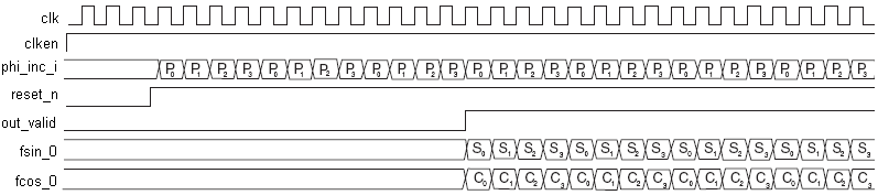
The phase increment for channel 0 is the first value read in on the rising edge of the clock following the de-assertion of reset_n (assuming clken is asserted) followed by the phase increments for the next (M-1) channels. The output signal out_valid is asserted when the first valid sine and cosine outputs for channel 0, S 0, C 0, respectively are available.
The output values S k and C k corresponding to channels 1 through (M-1) are output sequentially by the NCO. The outputs are interleaved so that a new output sample for channel k is available every M cycles.