F-Tile Avalon® Streaming Intel® FPGA IP for PCI Express* Design Example User Guide
ID
683372
Date
12/17/2021
Public
A newer version of this document is available. Customers should click here to go to the newest version.
2.1. Programmed Input/Output Design Example
2.2. Programmed Input/Output Design Example Functional Description
2.3. Programmed Input/Output Design Example Simulation Testbench
2.4. Single Root I/O Virtualization (SR-IOV) Design Example
2.5. Single Root I/O Virtualization (SR-IOV) Design Example Functional Description
2.6. Single Root I/O Virtualization (SR-IOV) Design Example Simulation Testbench
3.6.2. Running the SR-IOV Design Example
Here are the steps to test the SR-IOV design example on hardware:
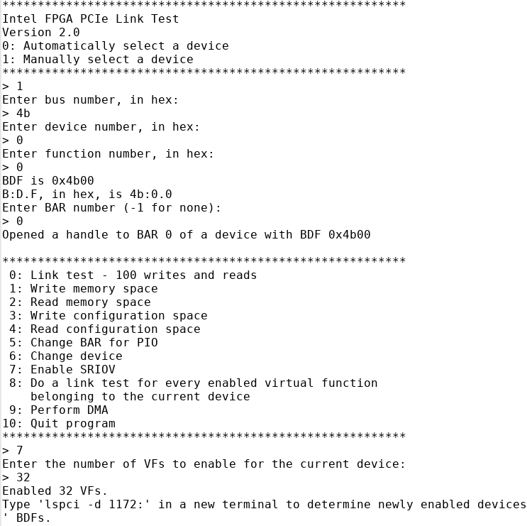
- Run the Intel FPGA IP PCIe link test by running the sudo ./intel_fpga_pcie_link_test command and then select the option 1: Manually select a device.
- Enter the BDF of the physical function for which the virtual functions are allocated.
- Enter BAR “0” to proceed to the test menu.
- Enter option 7 to enable SR-IOV for the current device.
- Enter the number of virtual functions to be enabled for the current device.
Figure 25. Link Test Menu

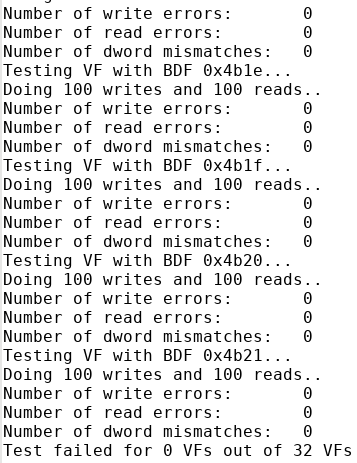
- Enter option 8 to perform a link test for every enabled virtual function allocated for the physical function. The link test application performs 100 memory writes with a single dword of data each and then reads the data back for checking. The application prints the number of virtual functions that failed the link test at the end of the testing.
Figure 26. Test Result

- In a new terminal, run the
command to verify the enumeration of PFs and VFs. The expected result is the sum of the number of physical functions and number of virtual functions.lspci –d 1172: | grep -c “Altera”Figure 27. lspci command