1.2. Generating the Design
Procedure
Example Design Tab in IP Parameter Editor
To create an Quartus® Prime Pro Edition project:
Follow these steps to generate the F-Tile CPRI PHY Intel® FPGA IP hardware design example and testbench:
- In the IP Catalog, locate and select F-Tile CPRI PHY Intel® FPGA IP. The New IP Variation dialog box appears.
- Specify a top-level name for your custom IP variation. The parameter editor saves the IP variation settings in a file named <your_ip> .ip.
- Click OK. The parameter editor appears.
- On the IP tab, specify the parameters for your IP core variation.
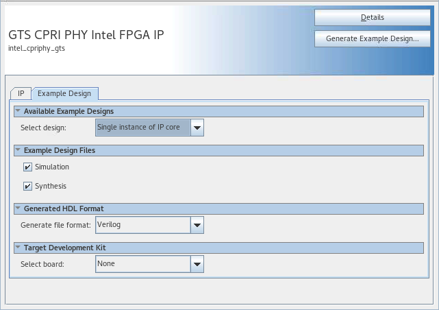
- On the Example Design tab, under Example Design Files, select the Simulation option to generate the testbench and the compilation-only project. Select the Synthesis option to generate the hardware design example. You must select at least one of the Simulation and Synthesis options to generate the design example.
- On the Example Design tab, under Generated HDL Format, select Verilog HDL or VHDL. If you select VHDL, you must simulate the testbench with a mixed-language simulator. The device under test in the ex_<datarate> directory is a VHDL model, but the main testbench file is a SystemVerilog file.
- Click the Generate Example Design button. The Select Example Design Directory dialog box appears.
- If you want to modify the design example directory path or name from the defaults (cpriphy_ftile_0_example_design), browse to the new path and type the new design example directory name (<design_example_dir>).
Figure 2. Analog Parameters Tab
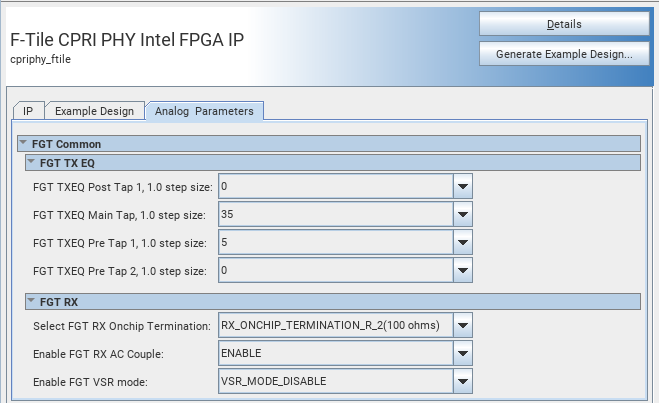
When the CPRI rate is 6.1440G and below, there are extra 3 analog parameters to configure:
- RXEQ VGA Gain
- RXEQ High Frequency Boost
- RXEQ DFE Data Tap1
Figure 3. For CPRI Rates 9.8304G and Above
Figure 4. For CPRI Rates 6.1440G and Below
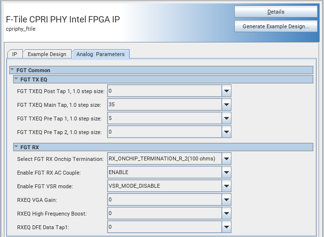
The default and recommended analog parameters values are shown in the table below:
| Parameter | Value |
|---|---|
| FGT TXEQ Post Tap 1, 1.0 step size | 0 |
| FGT TXEQ Main Tap 1.0 step size | 35 |
| FGT TXEQ Pre Tap 1, 1.0 step size | 5 |
| FGT TXEQ Pre Tap 2, 1.0 step size | 0 |
| FGT RX Onchip Termination | RX_ONCHIP_TERMINATION_R_2 (100 ohms) |
| Enable FGT RX AC Couple | ENABLE |
| Enable FGT VSR mode |
|
| RXEQ VGA Gain | 0 (Required only when CPRI rate is 6.1440Gbps and below) |
| RXEQ High Frequency Boost | 0 (Required only when CPRI rate is 6.1440Gbps and below) |
| RXEQ DFE Data Tap1 | 0 (Required only when CPRI rate is 6.1440Gbps and below) |
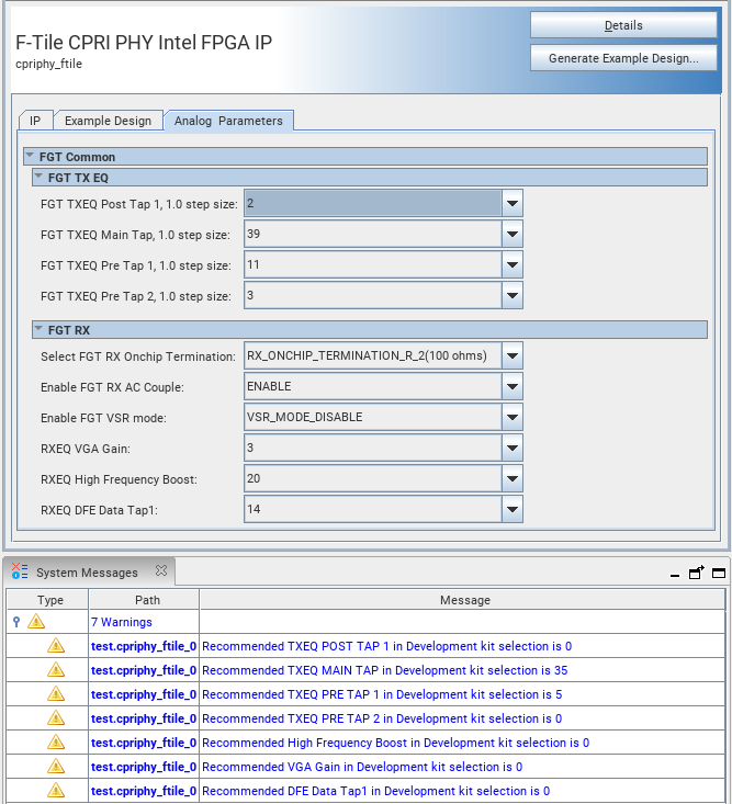
In the Example Design tab, if you select Target Development Kit to be Intel Agilex 7 FPGA I-Series Transceiver-SoC Development Kit, and you configure analog parameters other than the default and recommended values, you will see warnings to recommend you set to the default values.
Figure 5. Target Development Kit in the Example Design Tab
Figure 6. Warnings