AXI Streaming Intel® FPGA IP for PCI Express* User Guide
ID
790711
Date
4/12/2024
Public
A newer version of this document is available. Customers should click here to go to the newest version.
1. Introduction
2. Features
3. Getting Started with the AXI Streaming Intel® FPGA IP for PCI Express*
4. IP Architecture and Functional Description
5. AXI Streaming Intel® FPGA IP for PCI Express* Parameters
6. Interfaces and Signals
7. Register Descriptions
8. Document Revision History for the AXI Streaming Intel® FPGA IP for PCI Express* User Guide
A. Specifications
B. Simulating the Design Example
1.1. Goal of the AXI Streaming Intel® FPGA IP for PCI Express* User Guide
1.2. Intended Audience for the AXI Streaming Intel® FPGA IP for PCI Express* User Guide
1.3. What is PCI Express* ?
1.4. What are the Intel® FPGA IPs for PCI Express* ?
1.5. What is the AXI Streaming Intel® FPGA IP for PCI Express* ?
1.6. Example Use Models
1.7. Design Flow Requirements
3.1. Download and Install Quartus Software
3.2. Obtain and Install Intel FPGA IPs and Licenses
3.3. Configure and Generate the AXI Streaming Intel® FPGA IP for PCI Express*
3.4. Instantiate and Connect the AXI Streaming Intel® FPGA IP for PCI Express* Interfaces
3.5. Simulate the AXI Streaming Intel® FPGA IP for PCI Express* IP Variant
3.6. Compile the AXI Streaming Intel® FPGA IP for PCI Express* IP Variant
3.7. Software Drivers for AXI Streaming Intel® FPGA IP for PCI Express* IP Variant
3.8. Build the Application for the AXI Streaming Intel® FPGA IP for PCI Express* IP Variant
3.9. Verification with the AXI Streaming Intel® FPGA IP for PCI Express* IP Variant
3.10. Debugging with the AXI Streaming Intel® FPGA IP for PCI Express* IP Variant
4.1. Clocks and Resets
4.2. PCIe Hard IP (HIP)
4.3. HIP Interface (IF) Adaptor
4.4. Application Error Reporting
4.5. Debug Toolkit and Hard IP (HIP) Reconfiguration Interface
4.6. Configuration Space Extension
4.7. Control Shadow
4.8. Configuration Intercept Interface
4.9. Power Management
4.10. Legacy Interrupt
4.11. Credit Handling
4.12. Completion Timeout
4.13. Transaction Ordering
4.14. Page Request Service (PRS) Events
4.15. TX Non-Posted Metering Requirement on Application
4.16. MSI Pending
4.17. D-State Status
4.18. Configuration Retry Status Enable
4.19. AXI-Streaming Interface
4.20. Precision Time Measurement (PTM) [F/R-Tiles Only]
6.1. Overview
6.2. Clocks and Resets
6.3. Application Packet Interface
6.4. Configuration Extension Bus Interface
6.5. Configuration Intercept Interface
6.6. Function Level Reset Interface
6.7. Control Shadow Interface (st_ctrlshadow)
6.8. Completion Timeout Interface (st_cplto)
6.9. Miscellaneous Signals
6.10. Control and Status Register Responder Interface (lite_csr)
6.11. VF Error Flag Interface (vf_err/sent_vfnonfatalmsg)
6.12. VIRTIO PCI* Configuration Access Interface
6.13. Serial Data Signals
7.3.1.1. AXI Streaming Intel® FPGA IP for PCI Express* Version
7.3.1.2. AXI Streaming Intel® FPGA IP for PCI Express* Features
7.3.1.3. AXI Streaming Intel® FPGA IP for PCI Express* Interface Attributes
7.3.1.4. ERROR GEN CTRL
7.3.1.5. ERROR GEN ATTR
7.3.1.6. ERROR TLP Header DW0-3
7.3.1.7. ERROR TLP Prefix
7.3.1.8. HOT PLUG GEN CTRL
7.3.1.9. POWER MANAGEMENT CTRL
7.3.1.10. LEGACY INTERRUPT CTRL
7.3.1.11. CFG REG IA CTRL
7.3.1.12. CFG REG IA FN NUM
7.3.1.13. CFG REG IA WRDATA
7.3.1.14. CFG REG IA RDDATA
7.3.1.15. PRS CTRL
7.3.1.16. MSI PENDING CTRL
7.3.1.17. MSI PENDING
7.3.1.18. D-STATE STS
7.3.1.19. CFG RETRY CTRL
7.3.3.1. PERFMON CTRL
7.3.3.2. TX MRD TLP
7.3.3.3. TX MWR TLP
7.3.3.4. TX MSG TLP
7.3.3.5. TX CFGWR TLP
7.3.3.6. TX CFGRD TLP
7.3.3.7. RX MRD TLP
7.3.3.8. RX MWR TLP
7.3.3.9. RX MSG TLP
7.3.3.10. RX CFGWR TLP
7.3.3.11. RX CFGRD TLP
7.3.3.12. TX MEM DATA
7.3.3.13. TX CPL DATA
7.3.3.14. RX MEM DATA
7.3.3.15. RX CPL DATA
3.5.1. Simulating the Design Example
The simulation setup involves the use of a Root Port Bus Functional Model (BFM) to exercise the AXI Streaming Intel® FPGA IP for PCI Express* (DUT) as shown in the following figure.
Figure 8. PIO Design Example Simulation Testbench
The following flow diagram shows the steps to simulate the design example:
Figure 9. Procedure
- Change to the testbench simulation directory, <project_directory>/pcie_ss_ed_tb/pcie_ss_ed_tb/sim/<EDA_vendor>/simulator.
- Run the simulation script for the simulator of your choice. Refer to the table below.
- Analyze the results.
Note: The AXI Streaming Intel® FPGA IP for PCI Express* does not support parallel PIPE simulations.
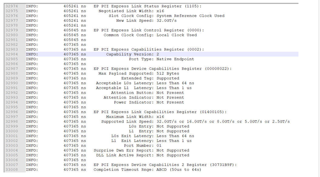
The following figure shows the link status information for a Gen5 x16 Endpoint simulation:
Figure 10. Link Status Information for a Gen5 x16 Endpoint Simulation
After a successful simulation, the simulation.log file contains a "successful completion" message.
This testbench simulates up to a Gen5 x16 variant.