AXI Streaming Intel® FPGA IP for PCI Express* User Guide
ID
790711
Date
4/12/2024
Public
A newer version of this document is available. Customers should click here to go to the newest version.
1. Introduction
2. Features
3. Getting Started with the AXI Streaming Intel® FPGA IP for PCI Express*
4. IP Architecture and Functional Description
5. AXI Streaming Intel® FPGA IP for PCI Express* Parameters
6. Interfaces and Signals
7. Register Descriptions
8. Document Revision History for the AXI Streaming Intel® FPGA IP for PCI Express* User Guide
A. Specifications
B. Simulating the Design Example
1.1. Goal of the AXI Streaming Intel® FPGA IP for PCI Express* User Guide
1.2. Intended Audience for the AXI Streaming Intel® FPGA IP for PCI Express* User Guide
1.3. What is PCI Express* ?
1.4. What are the Intel® FPGA IPs for PCI Express* ?
1.5. What is the AXI Streaming Intel® FPGA IP for PCI Express* ?
1.6. Example Use Models
1.7. Design Flow Requirements
3.1. Download and Install Quartus Software
3.2. Obtain and Install Intel FPGA IPs and Licenses
3.3. Configure and Generate the AXI Streaming Intel® FPGA IP for PCI Express*
3.4. Instantiate and Connect the AXI Streaming Intel® FPGA IP for PCI Express* Interfaces
3.5. Simulate the AXI Streaming Intel® FPGA IP for PCI Express* IP Variant
3.6. Compile the AXI Streaming Intel® FPGA IP for PCI Express* IP Variant
3.7. Software Drivers for AXI Streaming Intel® FPGA IP for PCI Express* IP Variant
3.8. Build the Application for the AXI Streaming Intel® FPGA IP for PCI Express* IP Variant
3.9. Verification with the AXI Streaming Intel® FPGA IP for PCI Express* IP Variant
3.10. Debugging with the AXI Streaming Intel® FPGA IP for PCI Express* IP Variant
4.1. Clocks and Resets
4.2. PCIe Hard IP (HIP)
4.3. HIP Interface (IF) Adaptor
4.4. Application Error Reporting
4.5. Debug Toolkit and Hard IP (HIP) Reconfiguration Interface
4.6. Configuration Space Extension
4.7. Control Shadow
4.8. Configuration Intercept Interface
4.9. Power Management
4.10. Legacy Interrupt
4.11. Credit Handling
4.12. Completion Timeout
4.13. Transaction Ordering
4.14. Page Request Service (PRS) Events
4.15. TX Non-Posted Metering Requirement on Application
4.16. MSI Pending
4.17. D-State Status
4.18. Configuration Retry Status Enable
4.19. AXI-Streaming Interface
4.20. Precision Time Measurement (PTM) [F/R-Tiles Only]
6.1. Overview
6.2. Clocks and Resets
6.3. Application Packet Interface
6.4. Configuration Extension Bus Interface
6.5. Configuration Intercept Interface
6.6. Function Level Reset Interface
6.7. Control Shadow Interface (st_ctrlshadow)
6.8. Completion Timeout Interface (st_cplto)
6.9. Miscellaneous Signals
6.10. Control and Status Register Responder Interface (lite_csr)
6.11. VF Error Flag Interface (vf_err/sent_vfnonfatalmsg)
6.12. VIRTIO PCI* Configuration Access Interface
6.13. Serial Data Signals
7.3.1.1. AXI Streaming Intel® FPGA IP for PCI Express* Version
7.3.1.2. AXI Streaming Intel® FPGA IP for PCI Express* Features
7.3.1.3. AXI Streaming Intel® FPGA IP for PCI Express* Interface Attributes
7.3.1.4. ERROR GEN CTRL
7.3.1.5. ERROR GEN ATTR
7.3.1.6. ERROR TLP Header DW0-3
7.3.1.7. ERROR TLP Prefix
7.3.1.8. HOT PLUG GEN CTRL
7.3.1.9. POWER MANAGEMENT CTRL
7.3.1.10. LEGACY INTERRUPT CTRL
7.3.1.11. CFG REG IA CTRL
7.3.1.12. CFG REG IA FN NUM
7.3.1.13. CFG REG IA WRDATA
7.3.1.14. CFG REG IA RDDATA
7.3.1.15. PRS CTRL
7.3.1.16. MSI PENDING CTRL
7.3.1.17. MSI PENDING
7.3.1.18. D-STATE STS
7.3.1.19. CFG RETRY CTRL
7.3.3.1. PERFMON CTRL
7.3.3.2. TX MRD TLP
7.3.3.3. TX MWR TLP
7.3.3.4. TX MSG TLP
7.3.3.5. TX CFGWR TLP
7.3.3.6. TX CFGRD TLP
7.3.3.7. RX MRD TLP
7.3.3.8. RX MWR TLP
7.3.3.9. RX MSG TLP
7.3.3.10. RX CFGWR TLP
7.3.3.11. RX CFGRD TLP
7.3.3.12. TX MEM DATA
7.3.3.13. TX CPL DATA
7.3.3.14. RX MEM DATA
7.3.3.15. RX CPL DATA
B.1.3. PIO Design Example Testbench
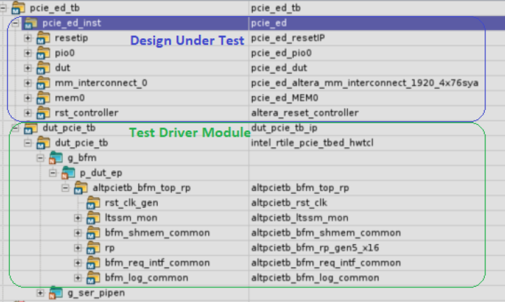
The figure below shows the PIO design example simulation design hierarchy. The tests for the PIO design example are defined with the apps_type_hwtcl parameter set to 3. The tests run under this parameter value are defined in ebfm_cfg_rp_ep_rootport, find_mem_bar and downstream_loop.
Figure 51. PIO Design Example Simulation Design Hierarchy
The testbench starts with link training and then accesses the configuration space of the IP for enumeration. A task called downstream_loop (defined in the Root Port PCIe BFM altpcietb_bfm_rp_gen5_x16.sv) then performs the PCIe link test. This test consists of the following steps:
- Issue a memory write command to write a single dword of data into the on-chip memory behind the Endpoint.
- Issue a memory read command to read back data from the on-chip memory.
- Compare the read data with the write data. If they match, the test counts this as a Pass.
- Repeat Steps 1, 2 and 3 for 10 iterations.
The first memory write takes place around 219 us. It is followed by a memory read at the Avalon® -ST RX interface of the Hard IP for PCIe. The Completion TLP appears shortly after the memory read request at the Avalon® -ST TX interface.
Note: In the 2x8 design example, memory read and memory write transactions are simulated on Port 0 only.