AN 976: JESD204C Intel® FPGA IP and ADI AD9081 MxFE* DAC Interoperability Report for Intel® Agilex® F-Tile Devices
1.4.2. Transmitter Transport Layer (TL)
To check the data integrity of the payload data stream through the transport layer, link layer and the PHY layer of the transmitter (TX) in JESD204C Intel® FPGA IP, the DAC is configured to PRBS23 test pattern. The DAC is also set to operate with the same configuration as set in the JESD204C Intel® FPGA IP. The PRBS generator in the JESD204C Intel® FPGA IP example design generates the PRBS23 pattern. The PRBS check in the DAC transport layer checks the PRBS23 data integrity.
The figure below shows the conceptual test setup for data integrity checking.
Figure 4. Data Integrity Check Using PRBS Checker
| Test Case | Objective | Description | Passing Criteria |
|---|---|---|---|
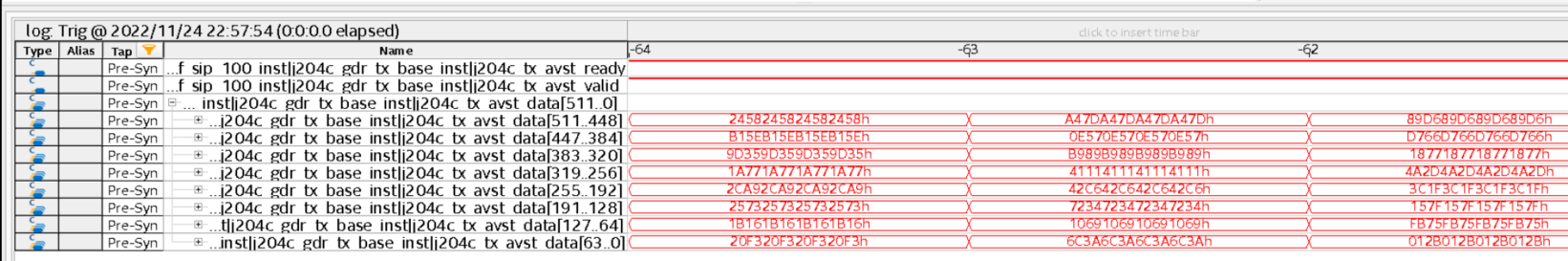
| TL.1 | Checks the transport layer mapping of the data channel using the PRBS23 test pattern. | The following signals in <ip_variant_name>_base.v is tapped:
The txframe_clk is used as the sampling clock for the Signal Tap. |
|
| TL.2 | Checks the data sample PRBS test using PRBS23 data. | Generated PRBS23 patterns from FPGA or transmitter are checked using AD9081 API functions. The tests performs the following steps:
The following registers in AD9081 are monitored for the PRBS23 test pattern:
|
Reading of datapath PRBS registers from 0x2063 to 0x2069 using the API functions as follows:
|
Figure 5. PRBS Pattern Diagram
2 M is the number of converters.
3 S is the number of transmitter samples per converter per frame.
4 WIDTH_MULP is the data width multiplier between the application layer and transport layer.
5 N is the number of conversion bits per converter.