AN 976: JESD204C Intel® FPGA IP and ADI AD9081 MxFE* DAC Interoperability Report for Intel® Agilex® F-Tile Devices
1.4.1. Transmitter Data Link Layer
This test area covers the test cases for tx_rst_n and link establishment.
On link start up, after tx_rst_n is deasserted, the JESD204C Intel® FPGA IP starts the link operation. In a typical user application, all run-time registers must be configured when the Avalon® memory-mapped configuration space is out of reset and before the txlink_clk and txframe_clk are out of reset. For link establishment with AD9081, the configuration is done through the API and jrx_dl_state is monitored to check the passing criteria link.
| Test Case | Objective | Description | Passing Criteria |
|---|---|---|---|
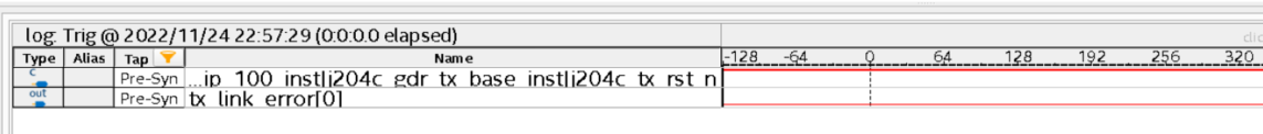
| LL.1 | Check if j204c_tx_rst_n is deasserted after the completion of the reset sequence. | The following signals in <ip_variant_name>_base.v is tapped:
|
|
| LL.2 | To verify link establishment from AD9081 after reset is released. This confirms sync header (SH) alignment and extended multiblock alignment completion. | The following signals from AD9081 are monitored for link establishment:
|
|
Note: j204c_tx_int is mapped to tx_link_error[0]. This tx_link_error[0] is captured in Signal Tap to verify the interrupt signal.
Figure 3. LL.1 Signal Tap Capture