A newer version of this document is available. Customers should click here to go to the newest version.
2.1.1. Constructing Communication Links in the Link Designer Module
2.1.2. Link and Simulation Setting
2.1.3. Transmitter Setting
2.1.4. Receiver Setting
2.1.5. IBIS-AMI Wrapper
2.1.6. Channel Setting
2.1.7. Batch Channel Simulation Configuration
2.1.8. Crosstalk Aggressor Transmitter Setting
2.1.9. Repeater and Retimer Configurations
2.1.10. Noise Source Link Component
2.1.11. System Options
2.1.12. Project Management Functions
2.1.13. Archiving and Unarchiving Projects
2.1.14. Device Model Importer
2.1.15. Analysis Functions and Pre-Simulation and Pre-Analysis Checklists
2.1.16. COM Analysis
3. Tutorial: PCI Express* 8GT
This tutorial uses Intel® Advanced Link Analyzer to run a link simulation. This example and its associated channel models are provided with the Intel® Advanced Link Analyzer distribution. The configuration file Demo.jne (included in the software distribution) contains the same link topology and a majority of the link settings discussed in this tutorial.
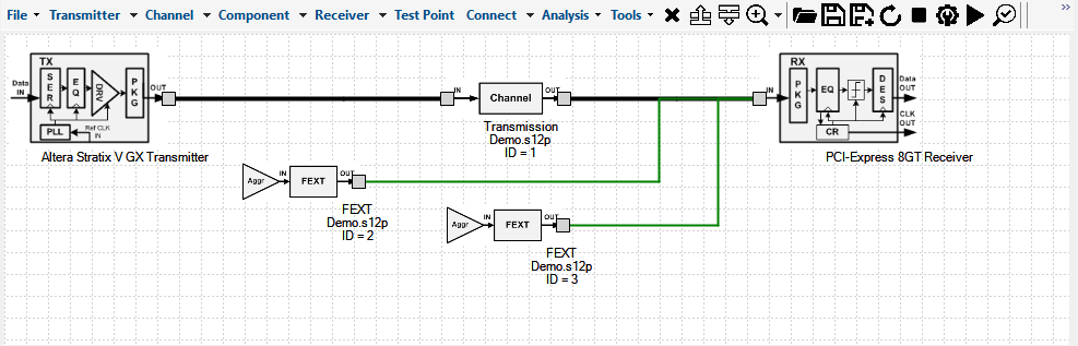
In this tutorial, a link that approximates a typical PCI Express* 8GT system with an Intel Stratix® V GX transmitter and a generic PCI Express* 8GT receiver is built and simulated in Intel® Advanced Link Analyzer. The following figure shows the link topology.
Note: This link configuration and simulation are for demonstration purposes. It is not intended for actual implementation. Consult Intel design guidelines for actual high-speed link design and implementation.
Figure 194. Example of PCI Express* 8GT Link Topology
Related Information