A newer version of this document is available. Customers should click here to go to the newest version.
5.6. Intel® FPGA PTC - DSP Page
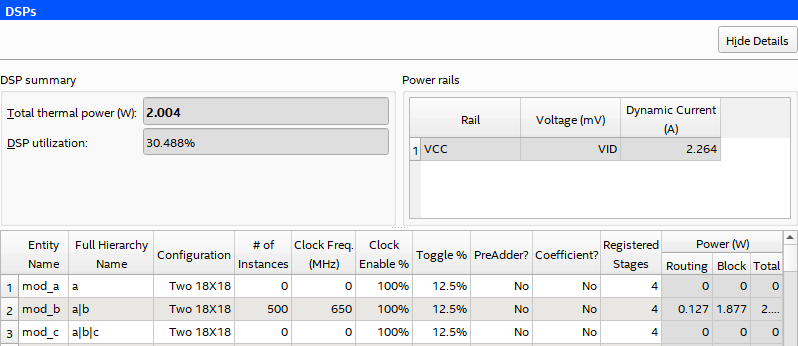
| Column Heading | Description | |
|---|---|---|
| Entity Name | Enter a name for the DSP entity in this column. This is an optional value. |
|
| Full Hierarchy Name | Specify the hierarchical path relevant to this entry. This is an optional entry. When entering levels of hierarchy, the pipe character (|) denotes a level of hierarchy. | |
| Configuration | Select the DSP block configuration for the module. | |
| # of Instances | Enter the number of DSP block instances that have the same configuration, clock frequency, toggle percentage, and register usage. This value is not necessarily equal to the number of dedicated DSP blocks you use. For example, it is possible to use two 18 × 18 simple multipliers that are implemented in the same DSP block in the FPGA devices. In this case, the number of instances would be two. To determine the maximum number of instances you can fit in the device for any particular mode, follow these steps:
|
|
| Clock Freq (MHz) | Enter the clock frequency for the module (in MHz). This value is limited by the maximum frequency specification for the device family. |
|
| Clock Enable % | Specifies the percentage of time that the DSP block is enabled. ( Intel® Agilex™ 7 devices only.) | |
| Toggle % | Enter the average percentage of DSP data outputs toggling on each clock cycle. The toggle percentage ranges from 0 to 50%. The default value is 12.5%. For a more conservative power estimate, use a higher toggle percentage. 50% corresponds to a randomly changing signal, since half the time the signal holds the same value and thus not transition. This is considered the highest meaningful toggle rate for a DSP block. |
|
| Preadder? | Select Yes if the PreAdder function of the DSP block is turned on. | |
| Coefficient? | Select Yes if the Coefficient function of the DSP block is turned on. | |
| Registered Stages | Select number of the registered stages. Permitted values depend on the selected mode; some modes, such as floating-point multiply and accumulate cannot have 0 register stages..
|
|
| Power (W) | Routing | Indicates the power dissipation due to estimated routing (in W). Routing power depends on placement and routing, which is a function of design complexity. The values shown represent the routing power estimate based on observed behavior across more than 100 real-world designs. |
| Block | Indicates the estimated power consumed by the DSP blocks (in W). |
|
| Total | Indicates the estimated power (in W), based on information entered into the Intel® FPGA PTC. It is the total power consumed by the DSP blocks and is equal to the routing power and block power. |
|
| User Comments | Enter any comments. This is an optional entry. | |