AN 943: Thermal Modeling for Intel® Stratix® 10 FPGAs with the Intel® FPGA Power and Thermal Calculator
6.2. Logic Design Information
Main Design Entry
The subject of this document is thermal analysis, therefore it focuses primarily on the thermal-related settings. For broader and more detailed information, refer to the Intel® FPGA Power and Thermal Calculator User Guide.
The following table shows values for the example using an 1SM21BE Intel® Stratix® 10 device.
| PTC Page | Values for this Design | Comment |
|---|---|---|
| Logic |
|
|
| RAM |
|
|
| DSP |
|
|
| Clock |
|
|
| PLL |
|
|
| I/O | Not assigned | None |
| I/O-IP | Not assigned | None |
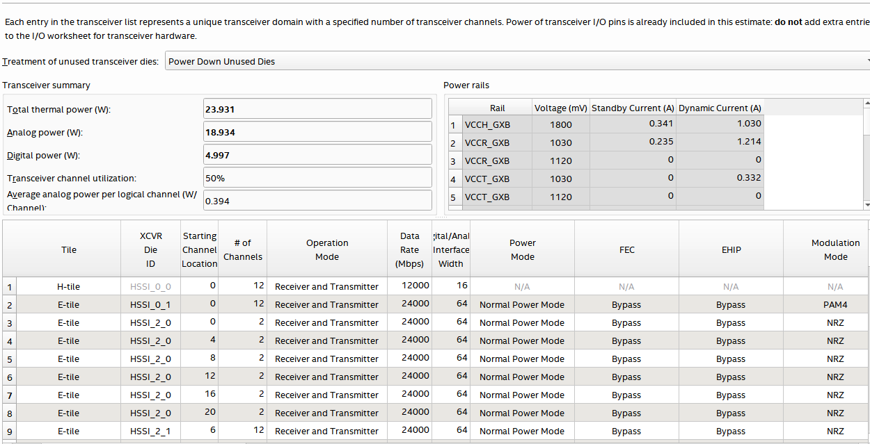
| Transceiver | In this example, 12 channels in each transceiver die are activated. | See the figure Transceiver Placements, below. |
| HPS | None | |
| HBM |
|

Determining Thermal Parameters
After you have completed your design entry, you must activate the Thermal page of the PTC, as follows:
- Set the Power characteristic field to Maximum.
- Set the Calculation Mode to Find a cooling solution for maximum junction temperature, or any other option other than the default.
With the Thermal page active, you must choose appropriate values for Calculation Mode, Recommended margin, and TSD mode:
- Calculation Mode. Choose one of the following:
- Use a constant junction temperature.
- This mode assumes that all junction temperatures are the same. This is usually not the case and should be used cautiously where the power calculated is too high and the PTC does not produce any thermal parameter for it.
- Enter the junction temperature in this mode.
- Find a cooling solution for a maximum junction temperature.
- Enter maximum TJ suitable for the design.
- Enter the ambient temperature.
- Find a maximum junction temperature for a cooling solution.
- Enter the ΨCA for your system's cooling solution.
- Enter the ambient temperature.
- Find an ambient temperature for a cooling solution.
- Enter the maximum TJ suitable for the design.
- Enter the ΨCA for the cooling solution.
- Use a constant junction temperature.
- Apply recommended margin. Choose one of the following:
- This field should be set to Yes if the power model status in the main page is not final. Turning it on almost adds over 20% to the total power of the FPGA and makes the thermal design very conservative. Consult your FAE and your system and circuit designers to determine the necessity of this option.
- If the power models are final it is not recommended to turn this field to yes. However, as the logic usage grows in the design process along with other uncertainties, it is a good practice to provide some cooling margin early in the thermal design. Keep in mind, any cooling design has a finite capacity and FPGA power dissipation can not grow over that. This can make it very difficult to add features later to the design if there was not any spare cooling to be tapped into.
- TSD mode. There are two sets of thermal sensors in the Intel® Stratix® 10 FPGA. Choose one from the dropped down menu in the thermal page:
- Using the Pinned out diodes (TSD), is where a set of sensors, one for each die are bonded out and only can be read by an outside device such as a Maxim 6581 or similar. These temperatures can be read while the FPGA is not active. In this mode the FPGA does not need to be on since the sensing is done by an outside device. For further detail on the bonded sensors and how to read them, refer to AN 769: Intel FPGA Remote Temperature Sensing Diode Implementation Guide
- Using DTS, with the temperature sensor IP, these are a set of sensors that are only readable through the Intel® Stratix® 10 Temperature IP Sense Software and only when the FPGA is on and instantiated. For more details on these sensors see Intel Stratix 10 Analog to Digital Converter user guide
These two sets of sensors do not coincide with each other nor necessarily with the hot spot on the die for a given design. Therefore the PTC provides two sets of offsets that need to be added to the sensor values read in the field, so the resulting temperatures are the maximum for the given die.
Note: The HBM temperature can be read only through the Intel® Stratix® 10 temperature IP sensor, and no offset value is required for it.