1.3. Generating the Design
Figure 4. Procedure
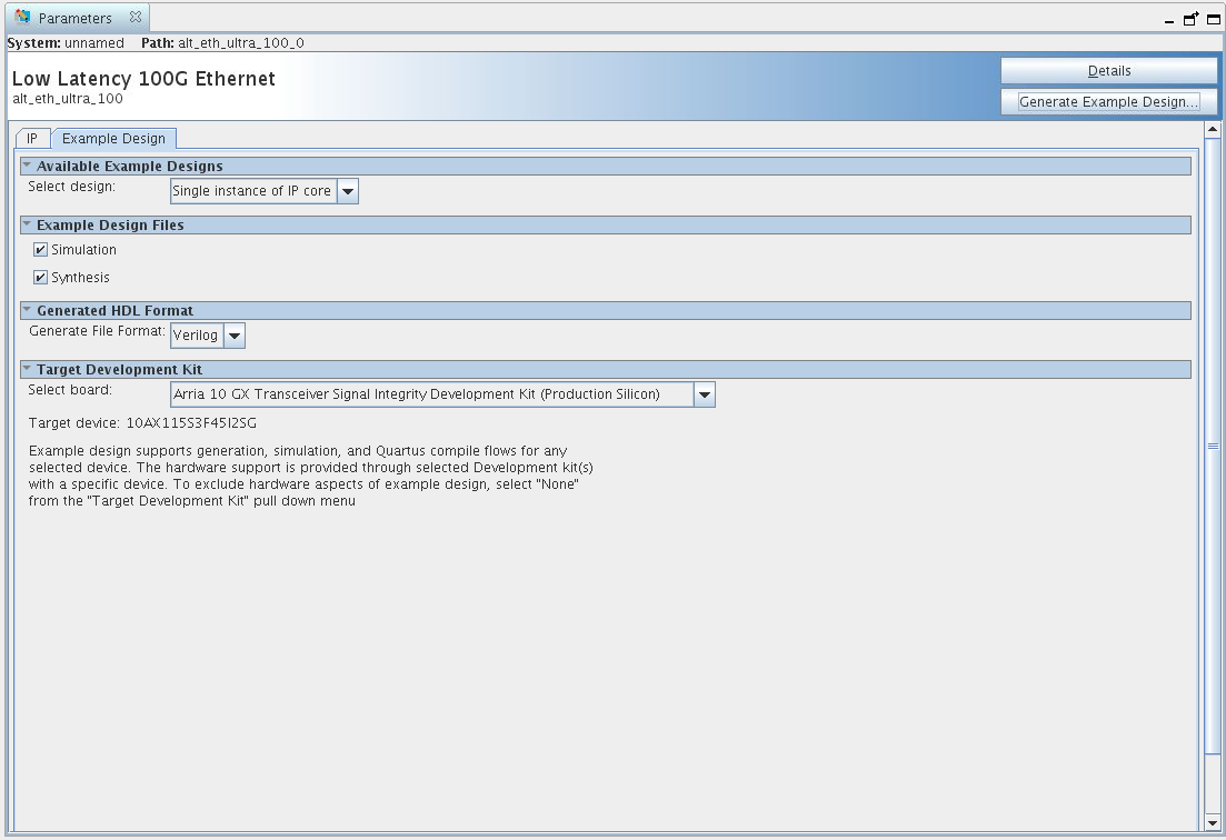
Figure 5. Example Design Tab in the LL 100GbE Parameter Editor
Follow these steps to generate the Arria 10 hardware design example and testbench:
- In the Quartus® Prime software, in the IP Catalog (), select the Arria 10 target device family.
Note: The hardware design example is only available in Arria 10 devices. The testbench is available for variations that target Arria 10 devices or Stratix V devices. For instructions to generate the testbench for Stratix V devices, refer to the IP core user guide.
- In the IP Catalog, locate and select Low Latency 100G Ethernet. The New IP Variation window appears.
- Specify a top-level name <your_ip> for your custom IP variation. The parameter editor saves the IP variation settings in a file named <your_ip> .qsys (in Quartus® Prime Standard Edition) or <your_ip> .ip (in Quartus® Prime Pro Edition).
- You must select a specific Arria 10 device in the Device field, or keep the default device the Quartus® Prime software proposes.
Note: The hardware design example overwrites the selection with the device on the target board. You specify the target board from the menu of design example options in the Example Design tab (Step 9).
- Click OK. The parameter editor appears.
- On the IP tab, specify the parameters for your IP core variation.
Note: The LL 100GbE design example is not available for the following selections:
- Use external MAC PLL
- Custom streaming client interface
- On the Example Design tab, under Example Design Files, select the Simulation option to generate the testbench, and select the Synthesis option to generate the compilation-only and hardware design examples.
Note: You must select at least one of the Simulation and Synthesis options to generate the design example.
- On the Example Design tab, under Generated HDL Format, only Verilog HDL is available. This IP core does not support VHDL.
- Under Target Development Kit select the Arria 10 GX Transceiver Signal Integrity Development Kit. The hardware example design overwrites the selection (in step 4) with the device on the target board.
- Click the Generate Example Design button. The Select Example Design Directory window appears.
- If you wish to modify the design example directory path or name from the defaults displayed ( alt_eth_ultra_100_0_example_design), browse to the new path and type the new design example directory name (<design_example_dir>).
- Refer to the KDB Answer How do I compensate for the jitter of PLL cascading or non-dedicated clock path for Arria 10 PLL reference clock? for a workaround you should apply in the hardware_test_design directory in the .sdc file.
Note: You must consult this KDB Answer because the RX path in the LL 100GbE IP core includes cascaded PLLs. Therefore, the IP core clocks might experience additional jitter in Arria 10 devices. This KDB Answer clarifies the software releases in which the workaround is necessary.